DS3908N+T&R Maxim Integrated Products, DS3908N+T&R Datasheet - Page 5
DS3908N+T&R
Manufacturer Part Number
DS3908N+T&R
Description
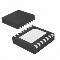
IC POT DUAL DIGITAL 14-TDFN
Manufacturer
Maxim Integrated Products
Datasheet
1.DS3908NTR.pdf
(11 pages)
Specifications of DS3908N+T&R
Taps
64
Resistance (ohms)
100K
Number Of Circuits
2
Temperature Coefficient
50 ppm/°C Typical
Memory Type
Non-Volatile
Interface
I²C, 2-Wire Serial
Voltage - Supply
3 V ~ 5.5 V
Operating Temperature
-40°C ~ 85°C
Mounting Type
Surface Mount
Package / Case
14-TDFN Exposed Pad
Resistance In Ohms
100K
Lead Free Status / RoHS Status
Lead free / RoHS Compliant


(T
A
TDFN PIN
-0.2
-0.4
-0.6
-0.8
-1.0
1.0
0.8
0.6
0.4
0.2
= +25°C, unless otherwise noted.)
3, 4, 5
10, 13
0
8, 11
9, 12
-40
14
NORMALIZED POT END-END RESISTANCE
1
2
6
7
V
CC
= 5V
-15
vs. TEMPERATURE
TEMPERATURE (°C)
A0, A1, A2
H0, H1
NAME
V0, V1
L0, L1
10
GND
SDA
SCL
V
WP
CC
-0.1
-0.2
-0.3
-0.4
-0.5
0.6
0.5
0.4
0.3
0.2
0.1
35
0
0.3
GAIN = 1V/V
DATA OFFSET TO SHOW 0 AT 2V CMV
Potentiometer with Buffered Outputs
vs. COMMON-MODE INPUT VOLTAGE
I
I
Address-Select Inputs. Determines I
Address and Address Pins section for more details.)
Write-Protect Input. Must be grounded to write to the registers. An internal pullup will lock the register
values if this pin is not connected.
Ground Terminal
Potentiometer Low Terminals. Voltages on these pins should remain between GND and V
Amplifier Outputs
Potentiometer High Terminals. Voltages on these pins should remain between GND and V
Supply Voltage Terminal
2
2
0.7
C Serial Data. Input/output for I
C Serial Clock. Input for I
Dual, 64-Position Nonvolatile Digital
60
COMMON-MODE INPUT VOLTAGE (V)
+85°C
+25°C
TYPICAL PGA OFFSET
1.1
-40°C
85
1.5
_____________________________________________________________________
1.9
-0.05
-0.10
-0.15
-0.20
-1.25
0.25
0.20
0.15
0.10
0.05
2.3
Typical Operating Characteristics (continued)
0
0
2.7
GAIN = 1V/V
IN
10
3.1
2
C clock.
POT INL vs. SETTING
3.5
POT0 SETTING (DEC)
20
2
C data.
2
30
C address. Device address is 1010A
-0.05
-0.15
0.25
0.15
0.05
-0.1
-0.2
0.2
0.1
0
40
-40
FUNCTION
CMV
50
CMV
-15
IN
TYPICAL PGA OFFSET
IN
= 2.0V
vs. TEMPERATURE
60
= 0.3V
CMV
TEMPERATURE (°C)
10
IN
= 3.5V
35
-0.05
-0.10
-0.15
-0.20
-1.25
0.25
0.20
0.15
0.10
0.05
0
0
60
GAIN = 1V/V
10
2
A
Pin Description
85
POT DNL vs. SETTING
1
A
POT0 SETTING (DEC)
20
0
. (See the I
30
CC
40
CC
2
.
C Slave
.
50
60
5
Related parts for DS3908N+T&R
Image
Part Number
Description
Manufacturer
Datasheet
Request
R

Part Number:
Description:
Digital Potentiometer ICs IC POT DUAL DIGITAL atile Digital Potent
Manufacturer:
Maxim Integrated Products
Datasheet:

Part Number:
Description:
Dual, 64-Position Nonvolatile Digital Potentiometer with Buffered Outputs
Manufacturer:
MAXIM [Maxim Integrated Products]
Datasheet:
Part Number:
Description:
Ds3908 Dual 64-position Nonvolatile Digital Potentiometer With Buffered Output
Manufacturer:
Maxim Integrated Products, Inc.
Datasheet:
Part Number:
Description:
MAX7528KCWPMaxim Integrated Products [CMOS Dual 8-Bit Buffered Multiplying DACs]
Manufacturer:
Maxim Integrated Products
Datasheet:
Part Number:
Description:
Single +5V, fully integrated, 1.25Gbps laser diode driver.
Manufacturer:
Maxim Integrated Products
Datasheet:
Part Number:
Description:
Single +5V, fully integrated, 155Mbps laser diode driver.
Manufacturer:
Maxim Integrated Products
Datasheet:
Part Number:
Description:
VRD11/VRD10, K8 Rev F 2/3/4-Phase PWM Controllers with Integrated Dual MOSFET Drivers
Manufacturer:
Maxim Integrated Products
Datasheet:
Part Number:
Description:
Highly Integrated Level 2 SMBus Battery Chargers
Manufacturer:
Maxim Integrated Products
Datasheet:
Part Number:
Description:
Current Monitor and Accumulator with Integrated Sense Resistor; ; Temperature Range: -40°C to +85°C
Manufacturer:
Maxim Integrated Products
Part Number:
Description:
TSSOP 14/A°/RS-485 Transceivers with Integrated 100O/120O Termination Resis
Manufacturer:
Maxim Integrated Products
Part Number:
Description:
TSSOP 14/A°/RS-485 Transceivers with Integrated 100O/120O Termination Resis
Manufacturer:
Maxim Integrated Products
Part Number:
Description:
QFN 16/A°/AC-DC and DC-DC Peak-Current-Mode Converters with Integrated Step
Manufacturer:
Maxim Integrated Products
Part Number:
Description:
TDFN/A/65V, 1A, 600KHZ, SYNCHRONOUS STEP-DOWN REGULATOR WITH INTEGRATED SWI
Manufacturer:
Maxim Integrated Products
Part Number:
Description:
Integrated Temperature Controller f
Manufacturer:
Maxim Integrated Products
Part Number:
Description:
SOT23-6/I°/45MHz to 650MHz, Integrated IF VCOs with Differential Output
Manufacturer:
Maxim Integrated Products