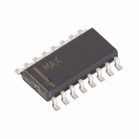
DS1882Z-050+T&R Maxim Integrated Products, DS1882Z-050+T&R Datasheet - Page 11

DS1882Z-050+T&R
Manufacturer Part Number
DS1882Z-050+T&R
Description
IC POT DIGIT DL LOG 50K 16SOIC
Manufacturer
Maxim Integrated Products
Datasheet
1.DS1882Z-050TR.pdf
(15 pages)
Specifications of DS1882Z-050+T&R
Taps
64
Resistance (ohms)
45K
Number Of Circuits
2
Temperature Coefficient
750 ppm/°C Typical
Memory Type
Non-Volatile
Interface
I²C, 2-Wire Serial
Voltage - Supply
4.5 V ~ 7 V
Operating Temperature
-40°C ~ 85°C
Mounting Type
Surface Mount
Package / Case
16-SOIC (3.9mm Width)
Resistance In Ohms
45K
Lead Free Status / RoHS Status
Lead free / RoHS Compliant
The CE pin serves as a communication enable pin.
When active (CE = 0), the inputs SDA and SCL are rec-
ognized by the device. If inactive (CE = 1), pins SDA
and SCL are disabled, making I
impossible.
Three pins, A0, A1, A2, serve as slave address inputs.
For multidrop configurations, they allow eight such
devices to be addressed by the same I
I
As shown in Figure 1, the DS1882 provides one read
command operation. This operation allows the user to
read both Potentiometer Wiper Setting Registers and
the Configuration Register. To initiate a read operation,
the R/W bit of the slave address byte is set to 1.
Communication to read the DS1882 begins with a
START condition, which is issued by the master device.
The slave address byte sent from the master device fol-
lows the START condition. Once a matching slave
address byte has been received by the DS1882, the
DS1882 responds with an acknowledge. The master
can then begin to receive data. The value of the wiper
Figure 1. Read Protocol
2
C address matches the hardware levels of these bits,
MSB
0
MSB
0
1 0 1
SLAVE ADDRESS
BYTE
I
A
2
2
C Interface for the DS1882
1
A
1
R/W = 1
A
0
LSB
Dual Log Audio Digital Potentiometer
1
Reading Pot Values
MSB
DATA BYTES ARE READ IN THE ORDER SHOWN ABOVE.
0
2
0
C communication
0
____________________________________________________________________
COMMAND
2
C bus. If the
BYTE
POT-0
SLAVE ADDRESS BYTE
LSB
1
READ PROTOCOL
MSB
0
the DS1882 is allowed to receive communications from
the I
The I
first byte transmitted from the master to the DS1882.
The upper nibble value is fixed to 0101. Bit values A2,
A1, and A0 are determined by the states of the corre-
sponding pins. The LSB, R/W, determines whether a
read or write will be performed.
The next byte to be transmitted is the Command Byte
(see the Command Byte section for details).
of Potentiometer 0 is the first returned from the DS1882.
It is then followed by the value of Potentiometer 1 and
then the value of the Configuration Register. Once the 8
bits of the Configuration Register have been sent, the
master needs to issue an acknowledge, unless it is the
last byte to be read, in which case the master issues a
not acknowledge. If desired, the master may stop the
communication transfer at this point by issuing the
STOP condition after the not acknowledge. However, if
the value of the three registers is needed again, the
transfer can continue by clocking the 8 bits of the
Potentiometer 0 value as described above.
1
A2
2
COMMAND
2
C bus.
C slave address byte is shown below. This is the
BYTE
POT-1
LSB
A1
MSB
1 0
COMMAND
BYTE
A0
CONFIG
REG
LSB
LSB
R/W
11


