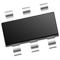
PIC10F322T-I/OT Microchip Technology, PIC10F322T-I/OT Datasheet - Page 114

PIC10F322T-I/OT
Manufacturer Part Number
PIC10F322T-I/OT
Description
896 B Flash, 64 B RAM, 4 I/O, 8bit ADC, PWM, CLC, DDS, CWG, TEMP Indicator, 2.3V
Manufacturer
Microchip Technology
Datasheet
1.PIC10F320-IOT.pdf
(210 pages)
Specifications of PIC10F322T-I/OT
Core
RISC
Processor Series
PIC10F
Data Bus Width
8 bit
Maximum Clock Frequency
31 KHz
Program Memory Size
512 B
Data Ram Size
64 B
Number Of Programmable I/os
4
Number Of Timers
2
Operating Temperature Range
- 40 C to + 85 C
Package / Case
SOT-23-6
Mounting Style
SMD/SMT
Maximum Operating Temperature
+ 85 C
Program Memory Type
Flash
Lead Free Status / Rohs Status
Details
Available stocks
Company
Part Number
Manufacturer
Quantity
Price
Company:
Part Number:
PIC10F322T-I/OT
Manufacturer:
VISHAY
Quantity:
11 490
Part Number:
PIC10F322T-I/OT
Manufacturer:
MICROCHIP/微芯
Quantity:
20 000
PIC10(L)F320/322
19.1
Programming the CLCx module is performed by config-
uring the four stages in the logic signal flow. The four
stages are:
• Data selection
• Data gating
• Logic function selection
• Output polarity
Each stage is setup at run time by writing to the corre-
sponding CLCx Special Function Registers. This has
the added advantage of permitting logic reconfiguration
on-the-fly during program execution.
19.1.1
There are eight signals available as inputs to the con-
figurable logic. Four 8-input multiplexers are used to
select the inputs to pass on to the next stage.
Data inputs are selected with the CLCxSEL0 and
CLCxSEL1 registers
respectively).
Data selection is through four multiplexers as indicated
on the left side of
are identified by a generic numbered input name.
Table 19-1
actual signal for each CLC module. The columns
labeled lcxd1 through lcxd4 indicate the MUX output for
the selected data input. D1S through D4S are
abbreviations for the MUX select input codes:
LCxD1S<2:0> through LCxD4S<2:0>, respectively.
Selecting a data input in a column excludes all other
inputs in that column.
TABLE 19-1:
DS41585A-page 114
CLCxIN[0]
CLCxIN[1]
CLCxIN[2]
CLCxIN[3]
CLCxIN[4]
CLCxIN[5]
CLCxIN[6]
CLCxIN[7]
Data Input
Note:
CLCx Setup
correlates the generic input name to the
DATA SELECTION
Data selections are undefined at power-up.
lcxd1
D1S
000
001
010
011
100
101
110
111
Figure
CLCx DATA INPUT
SELECTION
lcxd2
(Register 19-3
D2S
000
001
010
011
100
101
110
111
19-2. Data inputs in the figure
lcxd3
D3S
000
001
010
011
100
101
110
111
and
lcxd4
D4S
000
001
010
011
100
101
110
111
Register
CLCx
CLCxIN1
CLCxIN2
PWM1
PWM2
NCOx
F
LFINTOSC
OSC
CLC 1
19-4,
Preliminary
19.1.2
Outputs from the input multiplexers are directed to the
desired logic function input through the data gating
stage. Each data gate can direct any combination of the
four selected inputs.
The gate stage is more than just signal direction. The gate
can be configured to direct each input signal as inverted
or non-inverted data. Directed signals are ANDed
together in each gate. The output of each gate can be
inverted before going on to the logic function stage.
The gating is in essence a 1-to-4 input AND/NAND/OR/
NOR gate. When every input is inverted and the output
is inverted, the gate is an OR of all enabled data inputs.
When the inputs and output are not inverted, the gate
is an AND or all enabled inputs.
Table 19-2
obtained in gate 1 by using the gate logic select bits.
The table shows the logic of four input variables, but
each gate can be configured to use less than four. If no
inputs are selected, the output will be zero or one,
depending on the gate output polarity bit.
TABLE 19-2:
It is possible (but not recommended) to select both the
true and negated values of an input. When this is done,
the gate output is zero, regardless of the other inputs,
but may emit logic glitches (transient-induced pulses). If
the output of the channel must be zero or one, the
recommended method is to set all gate bits to zero and
use the gate polarity bit to set the desired level.
Data gating is configured with the logic gate select
registers as follows:
• Gate 1: CLCxGLS0
• Gate 2: CLCxGLS1
• Gate 3: CLCxGLS2
• Gate 4: CLCxGLS3
Register number suffixes are different than the gate
numbers because other variations of this module have
multiple gate selections in the same register.
Data gating is indicated in the right side of
Only one gate is shown in detail. The remaining three
gates are configured identically with the exception that
the data enables correspond to the enables for that gate.
Note:
CLCxGLS0
0xAA
0xAA
0x55
0x55
0x00
0x00
DATA GATING
Data gating is undefined at power-up.
summarizes the basic logic that can be
DATA GATING LOGIC
LCxGyPOL
(Register
(Register
(Register
(Register
1
0
1
0
0
1
2011 Microchip Technology Inc.
19-5)
19-6)
19-7)
19-8)
Gate Logic
Logic 0
Logic 1
NAND
NOR
AND
OR
Figure
19-2.


