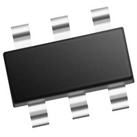
PIC10F322T-I/OT Microchip Technology, PIC10F322T-I/OT Datasheet - Page 115

PIC10F322T-I/OT
Manufacturer Part Number
PIC10F322T-I/OT
Description
896 B Flash, 64 B RAM, 4 I/O, 8bit ADC, PWM, CLC, DDS, CWG, TEMP Indicator, 2.3V
Manufacturer
Microchip Technology
Datasheet
1.PIC10F320-IOT.pdf
(210 pages)
Specifications of PIC10F322T-I/OT
Core
RISC
Processor Series
PIC10F
Data Bus Width
8 bit
Maximum Clock Frequency
31 KHz
Program Memory Size
512 B
Data Ram Size
64 B
Number Of Programmable I/os
4
Number Of Timers
2
Operating Temperature Range
- 40 C to + 85 C
Package / Case
SOT-23-6
Mounting Style
SMD/SMT
Maximum Operating Temperature
+ 85 C
Program Memory Type
Flash
Lead Free Status / Rohs Status
Details
Available stocks
Company
Part Number
Manufacturer
Quantity
Price
Company:
Part Number:
PIC10F322T-I/OT
Manufacturer:
VISHAY
Quantity:
11 490
Part Number:
PIC10F322T-I/OT
Manufacturer:
MICROCHIP/微芯
Quantity:
20 000
- Current page: 115 of 210
- Download datasheet (2Mb)
19.1.3
There are eight available logic functions including:
• AND-OR
• OR-XOR
• AND
• S-R Latch
• D Flip-Flop with Set and Reset
• D Flip-Flop with Reset
• J-K Flip-Flop with Reset
• Transparent Latch with Set and Reset
Logic functions are shown in
function has four inputs and one output. The four inputs
are the four data gate outputs of the previous stage. The
output is fed to the inversion stage and from there to other
peripherals, an output pin, and back to the CLCx itself.
19.1.4
The last stage in the configurable logic cell is the output
polarity. Setting the LCxPOL bit of the CLCxCON reg-
ister inverts the output signal from the logic stage.
Changing the polarity while the interrupts are enabled
will cause an interrupt for the resulting output transition.
2011 Microchip Technology Inc.
LOGIC FUNCTION
OUTPUT POLARITY
Figure
19-3. Each logic
Preliminary
19.1.5
The following steps should be followed when setting up
the CLCx:
• Disable CLCx by clearing the LCxEN bit.
• Select desired inputs using CLCxSEL0 and
• Clear any associated ANSEL bits.
• Set all TRIS bits associated with inputs.
• Clear all TRIS bits associated with outputs.
• Enable the chosen inputs through the four gates
• Select the gate output polarities with the
• Select the desired logic function with the
• Select the desired polarity of the logic output with
• If driving the CLCx pin, set the LCxOE bit of the
• If interrupts are desired, configure the following
• Enable the CLCx by setting the LCxEN bit of the
CLCxSEL1 registers (See
using CLCxGLS0, CLCxGLS1, CLCxGLS2, and
CLCxGLS3 registers.
LCxPOLy bits of the CLCxPOL register.
LCxMODE<2:0> bits of the CLCxCON register.
the LCxPOL bit of the CLCxPOL register. (This
step may be combined with the previous gate out-
put polarity step).
CLCxCON register and also clear the TRIS bit
corresponding to that output.
bits:
- Set the LCxINTP bit in the CLCxCON register
- Set the LCxINTN bit in the CLCxCON
- Set the CLCxIE bit of the associated PIE
- Set the GIE and PEIE bits of the INTCON
CLCxCON register.
for rising event.
register or falling event.
registers.
register.
PIC10(L)F320/322
CLCX SETUP STEPS
Table
19-1).
DS41585A-page 115
Related parts for PIC10F322T-I/OT
Image
Part Number
Description
Manufacturer
Datasheet
Request
R

Part Number:
Description:
896 B Flash, 64 B RAM, 4 I/O, 8bit ADC, PWM, CLC, DDS, CWG, TEMP Indicator, 2.3V
Manufacturer:
Microchip Technology

Part Number:
Description:
896 B Flash, 64 B RAM, 4 I/O, 8bit ADC, PWM, CLC, DDS, CWG, TEMP Indicator, 2.3V
Manufacturer:
Microchip Technology

Part Number:
Description:
896 B Flash, 64 B RAM, 4 I/O, 8bit ADC, PWM, CLC, DDS, CWG, TEMP Indicator, 2.3V
Manufacturer:
Microchip Technology

Part Number:
Description:
896 B Flash, 64 B RAM, 4 I/O, 8bit ADC, PWM, CLC, DDS, CWG, TEMP Indicator, 2.3V
Manufacturer:
Microchip Technology

Part Number:
Description:
896 B Flash, 64 B RAM, 4 I/O, 8bit ADC, PWM, CLC, DDS, CWG, TEMP Indicator, 2.3V
Manufacturer:
Microchip Technology

Part Number:
Description:
896 B Flash, 64 B RAM, 4 I/O, 8bit ADC, PWM, CLC, DDS, CWG, TEMP Indicator, 2.3V
Manufacturer:
Microchip Technology

Part Number:
Description:
384B Flash, 16B RAM, 4 I/O, 8bit ADC 6 SOT-23 BAG
Manufacturer:
Microchip Technology
Datasheet:

Part Number:
Description:
768B Flash, 23B RAM, 4 I/O, 8bit ADC 6 SOT-23 BAG
Manufacturer:
Microchip Technology
Datasheet:

Part Number:
Description:
384B Flash, 16B RAM, 4 I/O, 8bit ADC 6 SOT-23 BAG
Manufacturer:
Microchip Technology
Datasheet:

Part Number:
Description:
768B Flash, 23B RAM, 4 I/O, 8bit ADC 6 SOT-23 BAG
Manufacturer:
Microchip Technology
Datasheet:

Part Number:
Description:
PIC10F PROGRAMMER ADAPTER (SOT-23), PICKIT
Manufacturer:
Microchip Technology Inc.

Part Number:
Description:
Manufacturer:
Microchip Technology Inc.
Datasheet:

Part Number:
Description:
Manufacturer:
Microchip Technology Inc.
Datasheet:


