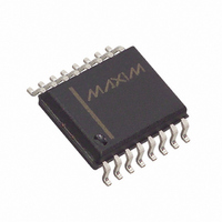
DS1807S+T&R Maxim Integrated Products, DS1807S+T&R Datasheet - Page 12

DS1807S+T&R
Manufacturer Part Number
DS1807S+T&R
Description
IC POT ADDRESS 2X AUDIO 16-SOIC
Manufacturer
Maxim Integrated Products
Datasheet
1.DS1807S.pdf
(13 pages)
Specifications of DS1807S+T&R
Taps
64
Resistance (ohms)
45K
Number Of Circuits
2
Temperature Coefficient
750 ppm/°C Typical
Memory Type
Volatile
Interface
I²C, 2-Wire Serial
Voltage - Supply
2.7 V ~ 5.5 V
Operating Temperature
-40°C ~ 85°C
Mounting Type
Surface Mount
Package / Case
16-SOIC (0.300", 7.5mm Width)
Resistance In Ohms
45K
Lead Free Status / RoHS Status
Lead free / RoHS Compliant
NOTES:
1. All voltages are referenced to ground.
2. I/O pins of fast mode devices must not obstruct the SDA and SCL lines if V
3. I
4. I
5. After this period, the first clock pulse is generated.
6. A device must internally provide a hold time of at least 300 ns for the SDA signal (referred to the
7. The maximum t
8. A fast mode device can be used in a standard mode system, but the requirement t
9. C
10. Absolute tolerance is used to determine measured wiper voltage versus expected wiper voltage as
11. Tap-to-tap tolerance is used to determine the change in voltage between successive tap positions. The
12. Typical values are for t
13. Address inputs, A0, A1, and A2, should be tied to either V
14. These parameters are characterized and not 100% tested.
15. Interchannel matching is used to determine the relative difference in dB between the same position on
16. See Figure 9.
17. Valid at 25 C only.
logic levels. I
inactive (high) states.
V
SCL signal.
then be met. This will automatically be the case if the device does not stretch the LOW period of the
SCL signal. If such a device does stretch the LOW period of the SCL signal, it must output the next
data bit to the SDA line t
determined by wiper position.
DS1807 is specified for a 0.25 dB tap-to-tap tolerance.
address selections.
each potentiometer. The DS1807 is specified for 0.5 dB Interchannel matching
CC
STBY
IHMIN
B
- total capacitance of one bus line in picofarads, timing referenced to (0.9(V
specified with zero-crossing detection active and operating device serial port in fast mode.
specified with for V
of the SCL signal) in order to bridge the undefined region of the falling edge of SCL.
STBY
HD:DAT
is specified as the current consumption of the device when SDA and SCL are in the
A
has only to be met if the device does not stretch the LOW period (t
= 25 C and nominal supply voltage.
RMAX
CC
equal 3.0V and 5.0V and SDA and SCL are driven to the appropriate
+ t
SU:DAT
= 1000+250=1250 ns before the SCL line is released.
12 of 13
CC
or GND depending on the desired
DD
is switched off.
CC
) and (0.1)(V
SU:DAT
> 250 ns must
110499
LOW
CC
) of the
DS1807
)).


