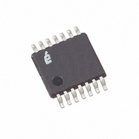
X9271UV14 Intersil, X9271UV14 Datasheet - Page 8

X9271UV14
Manufacturer Part Number
X9271UV14
Description
IC DIGITAL POT 50K 256TP 14TSSOP
Manufacturer
Intersil
Series
XDCP™r
Datasheet
1.X9271TV14ZT1.pdf
(22 pages)
Specifications of X9271UV14
Taps
256
Resistance (ohms)
50K
Number Of Circuits
1
Temperature Coefficient
300 ppm/°C Typical
Memory Type
Non-Volatile
Interface
SPI, 3-Wire Serial
Voltage - Supply
4.5 V ~ 5.5 V
Operating Temperature
0°C ~ 70°C
Mounting Type
Surface Mount
Package / Case
14-TSSOP
Resistance In Ohms
50K
Lead Free Status / RoHS Status
Contains lead / RoHS non-compliant
Available stocks
Company
Part Number
Manufacturer
Quantity
Price
Company:
Part Number:
X9271UV14Z
Manufacturer:
Intersil
Quantity:
1 000
DEVICE DESCRIPTION
Instructions
I
The first byte sent to the X9271 from the host,
following a CS going HIGH to LOW, is called the
Identification byte. The most significant four bits of the
slave address are a device type identifier. The ID[3:0]
bits is the device id for the X9271; this is fixed as
0101[B] (refer to Table 4).
The A1 - A0 bits in the ID byte is the internal slave
address. The physical device address is defined by the
state of the A1 - A0 input pins. The slave address is
externally specified by the user. The X9271 compares
the serial data stream with the address input state; a
successful compare of both address bits is required for
the X9271 to successfully continue the command
sequence. Only the device which slave address
matches the incoming device address sent by the
master executes the instruction. The A1 - A0 inputs
can be actively driven by CMOS input signals or tied to
V
I
The next byte sent to the X9271 contains the
instruction and register pointer information. The three
most significant bits are used provide the instruction
opcode (I[3:0]). The RB and RA bits point to one of the
four Data Registers. P0 is the POT selection; since the
X9271 is single POT, the P0=0. The format is shown in
Table 5.
R
There are 16 registers organized into four banks. Bank
0 is the default bank of registers. Only Bank 0 registers
can be used for data register to Wiper Counter
Register operations.
Table 4. Identification Byte Format
DENTIFICATION
NSTRUCTION
CC
EGISTER
(MSB)
or V
ID3
0
SS
B
.
ANK
B
YTE
ID2
B
1
S
YTE
Device Type
ELECTION
Identifier
(I[3:0])
(ID
AND
8
ID1
0
(R1, R0, P1, P0)
A)
ID0
1
for proper operation
0
X9271
Set to 0
Banks 1, 2, and 3 are additional banks of registers (12
total) that can be used for SPI write and read
operations. The data registers in Banks 1, 2, and 3
cannot be used for direct read/write operations
between the Wiper Counter Register.
Register Selection (DR0 to DR3) Table
Register Bank Selection (Bank 0 to Bank 3) Table
0
RB RA
P1
0
0
1
1
0
0
1
1
P0
0
1
0
1
0
1
0
1
A1
Selection
Selection
Register
Slave Address
Bank
Internal
0
1
2
3
0
1
2
3
(LSB)
A0
Data Register Read and Write;
Wiper Counter Register
Operations
Data Register Read and Write;
Wiper Counter Register
Operations
Data Register Read and Write;
Wiper Counter Register
Operations
Data Register Read and Write;
Wiper Counter Register
Operations
Data Register Read and Write;
Wiper Counter Register
Operations
Data Register Read and Write
Only
Data Register Read and Write
Only
Data Register Read and Write
Only
Operations
Operations
November 22, 2005
FN8174.2


