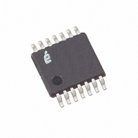
X93256UV14I-2.7T1 Intersil, X93256UV14I-2.7T1 Datasheet - Page 5

X93256UV14I-2.7T1
Manufacturer Part Number
X93256UV14I-2.7T1
Description
IC XDCP DUAL 32-TAP 50K 14-TSSOP
Manufacturer
Intersil
Series
XDCP™r
Datasheet
1.X93256UV14IZ-2.7.pdf
(7 pages)
Specifications of X93256UV14I-2.7T1
Taps
32
Resistance (ohms)
50K
Number Of Circuits
2
Temperature Coefficient
35 ppm/°C Typical
Memory Type
Non-Volatile
Interface
Up/Down (3-Wire)
Voltage - Supply
2.7 V ~ 5.5 V
Operating Temperature
-40°C ~ 85°C
Mounting Type
Surface Mount
Package / Case
14-TSSOP
Resistance In Ohms
50K
Lead Free Status / RoHS Status
Contains lead / RoHS non-compliant
AC Operating Characteristics
AC Timing
Power-up and Power-down Requirements
There are no restrictions on the power-up or power-down
conditions of V
potentiometer pins provided that V
positive than or equal to V
V
Pin Descriptions
In the text, CS, INC, U/D, R
to either CS
applied independently or at the same time.
R
The R
fixed terminals of a mechanical potentiometer. The minimum
voltage is V
R
relation to wiper movement direction selected by the U/D
input per potentiometer.
R
The R
potentiometer, which is equivalent to the movable terminal of
a mechanical potentiometer.
CC
H
W
H
SYMBOL
(Note 5)
(Note 5)
t
and R
R
t
and R
t
t
t
R
t
CPH
CPH
CYC
WR
ramp rate specification is always in effect.
t
V
lC
, t
W
H
CC
Note: CS, INC, U/D, R
to either CS
F
and R
pin of the X93256 is the wiper terminal of the
L
L
references the relative position of the terminal in
SS
1
INC
U/D
INC Inactive to CS Inactive
CS Deselect Time (No store)
CS Deselect Time (Store)
INC Cycle Time
INC Input Rise and Fall time
V CC Power-up Rate
Store Cycle
or CS
CS
L
CC
and the maximum is V
pins of the X93256 are equivalent to the
1
and the voltages applied to the
2
or CS
, etc. Note: These signals can be
t
CI
2
, etc.
H
H
H
and V
, R
and R
5
W
PARAMETER
, and R
L
CC
L
, i.e., V
are used to refer
Over recommended operating conditions, unless otherwise specified. In the table, CS, INC, U/D, R
R
t
IL
CC
L
is always more
t
ID
are used to refer to either CS
. The terminology of
t
CYC
L
CC
are used to refer
≥ V
t
IH
H,
V
L
. The
t
DI
X93256
t
IC
1
or CS
(Note 7)
Up/Down (U/D)
The U/D input controls the direction of a single
potentiometer’s wiper movement and whether the counter is
incremented or decremented.
Increment (INC)
The INC input is negative-edge triggered. Toggling INC will
move the wiper and either increment or decrement the
pertaining potentiometer’s counter in the direction indicated
by the logic level on the pertaining potentiometer’s U/D
input.
Chip Select (CS)
A potentiometer is selected when the pertaining CS input is
LOW. Its current counter value is stored in nonvolatile memory
when the pertaining CS is returned HIGH while the pertaining
INC input is also HIGH. After the store operation is complete
the affected potentiometer will be placed in the low power
standby mode until the potentiometer is selected once again.
Principles of Operation
There are multiple sections for each potentiometer in the
X93256: an input control, a counter and decode section; the
nonvolatile memory; and a resistor array. Each input control
MIN
250
0.2
2
10
1
2
, etc. (Continued)
(STORE)
t
CPH
(Note 4)
TYP
5
t
F
90%
10%
(Note 7)
MAX
90%
500
50
10
t
R
February 1, 2008
UNIT
V/ms
ms
ms
µs
ns
µs
µs
FN8188.2
H
and


