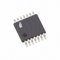
X9420WV14-2.7T1 Intersil, X9420WV14-2.7T1 Datasheet - Page 5

X9420WV14-2.7T1
Manufacturer Part Number
X9420WV14-2.7T1
Description
IC XDCP SGL 64-TAP 10K 14-TSSOP
Manufacturer
Intersil
Series
XDCP™r
Datasheet
1.X9420WV14I-2.7.pdf
(19 pages)
Specifications of X9420WV14-2.7T1
Taps
64
Resistance (ohms)
10K
Number Of Circuits
1
Temperature Coefficient
300 ppm/°C Typical
Memory Type
Non-Volatile
Interface
SPI, 3-Wire Serial
Voltage - Supply
2.7 V ~ 5.5 V
Operating Temperature
0°C ~ 70°C
Mounting Type
Surface Mount
Package / Case
14-TSSOP
Resistance In Ohms
10K
Lead Free Status / RoHS Status
Contains lead / RoHS non-compliant
Figure 1. Detailed Potentiometer Block Diagram
Write in Process
The contents of the Data Registers are saved to
nonvolatile memory when the CS pin goes from LOW to
HIGH after a complete write sequence is received by
the device. The progress of this internal write operation
can be monitored by a Write In Process bit (WIP). The
WIP bit is read with a Read Status command.
INSTRUCTIONS
Address/Identification (ID) Byte
The first byte sent to the X9420 from the host,
following a CS going HIGH to LOW, is called the
Address or Identification byte. The most significant
four bits of the slave address are a device type
identifier, for the X9420 this is fixed as 0101[B] (refer
to Figure 2).
The least significant bit in the ID byte selects one of
two devices on the bus. The physical device address
is defined by the state of the A
compares the serial data stream with the address
input state; a successful compare of the address bit is
required for the X9420 to successfully continue the
command sequence. The A
driven by a CMOS input signal or tied to V
The remaining three bits in the ID byte must be set to 110.
IF WCR = 00[H] THEN V
IF WCR = 3F[H] THEN V
Serial Data Path
From Interface
Circuitry
W
W
5
= V
= V
0
L
H
0
REGISTER 2
input can be actively
Register 0
input pin. The X9420
CC
8
or V
SS
REGISTER 3
Register 1
.
Modified SCK
X9420
UP/DN
6
Figure 2. Address/Identification Byte Format
Instruction Byte
The next byte sent to the X9420 contains the
instruction and register pointer information. The four
most significant bits are the instruction. The next two
bits point to one of four data registers. The format is
shown below in Figure 3.
Figure 3. Instruction Byte Format
UP/DN
CLK
Parallel
Serial
Bus
Input
Bus
Input
0
I3
Register
INC/DEC
Device Type
Counter
(WCR)
Wiper
Logic
Identifier
1
Instructions
I2
0
I1
C
O
U
N
T
E
R
D
E
C
O
D
E
1
I0
1
Register
R1
Select
1
R0
Device Address
0
0
A0
V
V
V
H
L
W
0
April 26, 2006
FN8195.1


