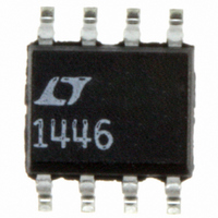
LTC1446CS8#PBF Linear Technology, LTC1446CS8#PBF Datasheet - Page 3

LTC1446CS8#PBF
Manufacturer Part Number
LTC1446CS8#PBF
Description
IC D/A CONV 12BIT R-R DUAL 8SOIC
Manufacturer
Linear Technology
Datasheet
1.LTC1446CN8PBF.pdf
(12 pages)
Specifications of LTC1446CS8#PBF
Settling Time
14µs
Number Of Bits
12
Data Interface
Serial
Number Of Converters
2
Voltage Supply Source
Single Supply
Power Dissipation (max)
5mW
Operating Temperature
0°C ~ 70°C
Mounting Type
Surface Mount
Package / Case
8-SOIC (3.9mm Width)
Number Of Channels
2
Resolution
12b
Interface Type
Serial (3-Wire)
Single Supply Voltage (typ)
5V
Dual Supply Voltage (typ)
Not RequiredV
Power Supply Requirement
Single
Output Type
Voltage
Integral Nonlinearity Error
5LSB
Single Supply Voltage (min)
4.5V
Single Supply Voltage (max)
5.5V
Dual Supply Voltage (min)
Not RequiredV
Dual Supply Voltage (max)
Not RequiredV
Operating Temp Range
0C to 70C
Operating Temperature Classification
Commercial
Mounting
Surface Mount
Pin Count
8
Package Type
SOIC N
Lead Free Status / RoHS Status
Lead free / RoHS Compliant
Available stocks
Company
Part Number
Manufacturer
Quantity
Price
ELECTRICAL CHARACTERISTICS
The
(LTC1446L), V
The
T
SYMBOL
Digital I/O
V
V
V
V
I
C
Switching
t
t
t
t
t
t
t
t
t
Note 1: Absolute Maximum Ratings are those values beyond which the life
of a device may be impaired.
Note 2: Nonlinearity is defined from the first code that is greater than or
equal to the maximum offset specification to code 4095 (full scale).
Note 3: Load is 5k in parallel with 100pF.
SYMBOL
Op Amp DC Performance
AC Performance
LEAK
1
2
3
4
5
6
7
8
9
A
IH
IL
OH
OL
IN
= T
MIN
denotes the specifications which apply over the full operating temperature range. V
denotes the specifications which apply over the full operating temperature range.V
to T
PARAMETER
Digital Input High Voltage
Digital Input Low Voltage
Digital Output High Voltage
Digital Output Low Voltage
Digital Input Leakage
Digital Input Capacitance
D
D
CLK High Time
CLK Low Time
CS/LD Pulse Width
LSB CLK to CS/LD
CS/LD Low to CLK
D
CLK Low to CS/LD Low
MAX,
PARAMETER
Short-Circuit Current Low
Short-Circuit Current High
Output Impedance to GND
Voltage Output Slew Rate
Voltage Output Settling Time
IN
IN
OUT
OUT A
Valid to CLK Setup
Valid to CLK Hold
Output Delay
unless otherwise noted.
and V
OUT B
unloaded, T
CONDITIONS
I
I
V
Guaranteed by Design
C
OUT
OUT
IN
LOAD
= GND to V
A
= – 1mA
= 1mA
= T
= 15pF
MIN
to T
CC
CONDITIONS
V
V
Input Code = 0
(Note 3)
(Notes 3, 4) to 0.5LSB
OUT
OUT
MAX,
Shorted to GND
Shorted to V
unless otherwise noted.
CC
Note 4: DAC switched between all 1s and the code corresponding to V
for the part.
Note 5: Digital inputs at 0V or V
V
CC
MIN
2.4
40
40
40
50
40
20
20
0
– 1.0
CC
CC
LTC1446
= 5V (LTC1446), V
TYP
= 4.5V to 5.5V (LTC1446), 2.7V to 5.5V
LTC1446/LTC1446L
CC
MAX
150
.
0.8
0.4
10
10
MIN
0.5
V
CC
MIN
60
60
60
80
60
30
30
2
0
– 0.7
CC
TYP
55
70
40
14
LTC1446L
1
= 3V (LTC1446L),
TYP
MAX
120
120
160
MAX
220
0.6
0.4
10
10
UNITS
UNITS
3
OS
V/ s
mA
mA
pF
ns
ns
ns
ns
ns
ns
ns
ns
ns
V
V
V
V
A
s


