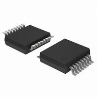
UDA1330ATS/N2,112 NXP Semiconductors, UDA1330ATS/N2,112 Datasheet - Page 8

UDA1330ATS/N2,112
Manufacturer Part Number
UDA1330ATS/N2,112
Description
IC AUDIO DAC STEREO 16-SSOP
Manufacturer
NXP Semiconductors
Datasheet
1.UDA1330ATSN2118.pdf
(23 pages)
Specifications of UDA1330ATS/N2,112
Number Of Bits
20
Data Interface
Serial
Number Of Converters
2
Voltage Supply Source
Analog and Digital
Power Dissipation (max)
75mW
Operating Temperature
-40°C ~ 85°C
Mounting Type
Surface Mount
Package / Case
16-SSOP
Lead Free Status / RoHS Status
Lead free / RoHS Compliant
Settling Time
-
Other names
568-3442-5
935262880112
UDA1330ATSDK
935262880112
UDA1330ATSDK
NXP Semiconductors
L3 INTERFACE
The following system and digital sound processing
features can be controlled in the L3 mode of the
UDA1330ATS:
• System clock frequency
• Data input format
• De-emphasis for 32, 44.1 and 48 kHz
• Volume
• Soft mute.
The exchange of data and control information between the
microcontroller and the UDA1330ATS is accomplished
through a serial interface comprising the following signals:
• L3DATA
• L3MODE
• L3CLOCK.
Information transfer through the microcontroller bus is
organized in accordance with the L3 interface format, in
which two different modes of operation can be
distinguished: address mode and data transfer mode.
Address mode
The address mode (see Fig.4) is required to select a
device communicating via the L3 interface and to define
the destination registers for the data transfer mode.
Data bits 7 to 2 represent a 6-bit device address where
bit 7 is the MSB. The address of the UDA1330ATS is
000101 (bit 7 to bit 2). If the UDA1330ATS receives a
different address, it will deselect its microcontroller
interface logic.
Data transfer mode
The selected address remains active during subsequent
data transfers until the UDA1330ATS receives a new
address command.
2001 Feb 02
Low-cost stereo filter DAC
8
The fundamental timing of data transfers (see Fig.5) is
essentially the same as the address mode. The maximum
input clock frequency and data rate is 64f
Data transfer can only be in one direction, consisting of
input to the UDA1330ATS to program sound processing
and other functional features. All data transfers are by 8-bit
bytes. Data will be stored in the UDA1330ATS after
reception of a complete byte.
A multibyte transfer is illustrated in Fig.6.
Registers
The sound processing and other feature values are stored
in independent registers. The first selection of the registers
is achieved by the choice of data type that is transferred.
This is performed in the address mode using bit 1 and bit 0
(see Table 5).
Table 5 Selection of data transfer
The second selection is performed by the 2 MSBs of the
data byte (bit 7 and bit 6). The other bits in the data byte
(bit 5 to bit 0) represent the value that is placed in the
selected registers.
The ‘status’ settings are given in Table 6 and the ‘data’
settings are given in Table 7.
BIT 1
0
0
1
1
BIT 0
0
1
0
1
data (volume, de-emphasis, mute)
not used
status (system clock frequency,
data input format)
not used
TRANSFER
UDA1330ATS
Product specification
s
.


