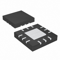
MAX5531ETC+ Maxim Integrated Products, MAX5531ETC+ Datasheet - Page 2

MAX5531ETC+
Manufacturer Part Number
MAX5531ETC+
Description
IC DAC 12BIT SGL ULP 12-TQFN
Manufacturer
Maxim Integrated Products
Datasheet
1.MAX5531ETC.pdf
(19 pages)
Specifications of MAX5531ETC+
Settling Time
660µs
Number Of Bits
12
Data Interface
MICROWIRE™, QSPI™, Serial, SPI™
Number Of Converters
1
Voltage Supply Source
Single Supply
Power Dissipation (max)
1.35mW
Operating Temperature
-40°C ~ 85°C
Mounting Type
Surface Mount
Package / Case
12-TQFN Exposed Pad
Number Of Dac Outputs
1
Resolution
12 bit
Interface Type
Serial (SPI)
Supply Voltage (max)
5.5 V
Supply Voltage (min)
1.8 V
Maximum Operating Temperature
+ 85 C
Mounting Style
SMD/SMT
Minimum Operating Temperature
- 40 C
Supply Current
0.007 mA
Voltage Reference
Internal
Lead Free Status / RoHS Status
Lead free / RoHS Compliant
ABSOLUTE MAXIMUM RATINGS
V
OUT to GND ...............................................-0.3V to (V
FB to GND ..................................................-0.3V to (V
SCLK, DIN,
REFIN, REFOUT to GND ............................-0.3V to (V
Continuous Power Dissipation (T
Ultra-Low-Power, 12-Bit,
Voltage-Output DACs
ELECTRICAL CHARACTERISTICS
(V
2
Stresses beyond those listed under “Absolute Maximum Ratings” may cause permanent damage to the device. These are stress ratings only, and functional
operation of the device at these or any other conditions beyond those indicated in the operational sections of the specifications is not implied. Exposure to
absolute maximum rating conditions for extended periods may affect device reliability.
STATIC ACCURACY (MAX5530 EXTERNAL REFERENCE)
Resolution
Integral Nonlinearity (Note 1)
Differential Nonlinearity (Note 1)
Offset Error (Note 2)
Offset-Error Temperature Drift
Gain Error (Note 3)
Gain-Error Temperature
Coefficient
Power-Supply Rejection Ratio
STATIC ACCURACY (MAX5531 INTERNAL REFERENCE)
Resolution
Integral Nonlinearity (Note 1)
Differential Nonlinearity (Note 1)
Offset Error (Note 2)
Offset-Error Temperature Drift
Gain Error (Note 3)
Gain-Error Temperature
Coefficient
DD
DD
Thin QFN (derate 16.9mW/°C above +70°C ..............1349mW
_______________________________________________________________________________________
to GND ..............................................................-0.3V to +6V
= +1.8V to +5.5V, OUT unloaded, T
PARAMETER
CS to GND ..............................-0.3V to (V
A
= +70°C)
SYMBOL
PSRR
DNL
DNL
V
V
INL
INL
GE
GE
A
N
N
OS
OS
= T
MIN
V
V
Guaranteed monotonic,
V
Guaranteed monotonic,
V
V
V
V
V
1.8V
V
V
Guaranteed monotonic,
V
Guaranteed monotonic,
V
V
V
V
V
to T
DD
DD
DD
DD
DD
DD
DD
DD
DD
DD
DD
DD
DD
DD
DD
DD
DD
DD
DD
DD
MAX
= 5V, V
= 1.8V, V
= 5V, V
= 1.8V, V
= 5V, V
= 1.8V, V
= 5V, V
= 1.8V, V
= 5V, V
= 1.8V, V
= 5V, V
= 1.8V, V
= 5V, V
= 1.8V, V
= 5V, V
= 1.8V, V
+ 0.3V)
+ 0.3V)
+ 0.3V)
+ 0.3V)
V
DD
, unless otherwise noted. Typical values are at T
REF
REF
REF
REF
REF
REF
REF
REF
5.5V
REF
REF
REF
REF
REF
REF
REF
REF
CONDITIONS
= 4.096V
= 4.096V
= 4.096V
= 4.096V
= 3.9V
= 3.9V
= 3.9V
= 3.9V
= 1.024V
= 1.024V
= 1.024V
= 1.024V
= 1.2V
= 1.2V
= 1.2V
= 1.2V
Operating Temperature Range ...........................-40°C to +85°C
Storage Temperature Range .............................-65°C to +150°C
Junction Temperature ..................................................... +150°C
Lead Temperature (soldering, 10s) .................................+300°C
MIN
12
12
A
±0.2
±0.2
±0.2
±0.2
TYP
±4
±4
±1
±1
±2
±2
±2
±4
±4
±4
±1
±1
±2
±2
±2
±4
85
= +25°C.)
MAX
±20
±20
±20
±20
±8
±8
±1
±1
±4
±4
±8
±8
±1
±1
±4
±4
ppm/ C
ppm/ C
UNITS
µV/ C
µV/ C
LSB
LSB
LSB
LSB
LSB
LSB
Bits
Bits
mV
mV
dB


