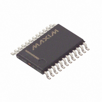
MAX5590BEUG+ Maxim Integrated Products, MAX5590BEUG+ Datasheet - Page 26

MAX5590BEUG+
Manufacturer Part Number
MAX5590BEUG+
Description
IC DAC 12BIT OCTAL BUFF 24-TSSOP
Manufacturer
Maxim Integrated Products
Datasheet
1.MAX5590BEUG.pdf
(33 pages)
Specifications of MAX5590BEUG+
Settling Time
3µs
Number Of Bits
12
Data Interface
Serial
Number Of Converters
8
Voltage Supply Source
Analog and Digital
Operating Temperature
-40°C ~ 85°C
Mounting Type
Surface Mount
Package / Case
24-TSSOP
Resolution
12 bit
Interface Type
Serial (SPI)
Supply Voltage (max)
5.25 V
Supply Voltage (min)
2.7 V
Maximum Operating Temperature
+ 85 C
Mounting Style
SMD/SMT
Minimum Operating Temperature
- 40 C
Supply Current
3.2 mA
Voltage Reference
External
Lead Free Status / RoHS Status
Lead free / RoHS Compliant
Power Dissipation (max)
-
Lead Free Status / Rohs Status
Lead free / RoHS Compliant
The MAX5590–MAX5595 provide two user-programma-
ble input/output (UPIO) ports: UPIO1 and UPIO2. These
ports have 15 possible configurations, as shown in
Table 22. UPIO1 and UPIO2 can be programmed inde-
pendently or simultaneously by writing to the UPSL1,
UPSL2, and UP0–UP3 bits (Table 18).
Table 19 shows how UPIO1 and UPIO2 are selected for
configuration. The UP0–UP3 bits select the desired
functions for UPIO1 and/or UPIO2 (Table 22).
Buffered, Fast-Settling, Octal, 12/10/8-Bit,
Voltage-Output DACs
Table 18. UPIO Write Command
X = Don’t care.
Table 19. UPIO Selection Bits (UPSL1 and UPSL2)
Table 20. UPIO Programming Example
X = Don’t care.
Table 21. UPIO Read Command
DOUTRB
X = Don’t care.
26
DATA
DATA
DATA
DIN
DIN
DIN
______________________________________________________________________________________
1
1
1
X
UPSL2
CONTROL BITS
CONTROL BITS
0
0
1
1
CONTROL BITS
UPIO Bits (UPSL1, UPSL2, UP0–UP3)
0
0
0
X
1
1
X
1
1
1
1
X
0
0
0
X
UPSL1
0
1
0
1
1
1
1
X
1
1
1
X
0
0
X
1
UPIO Programming Example:
To set only UPIO1 as LDAC and leave UPIO2
unchanged, use the command in Table 20.
The UPIO selection and configuration bits can be read
back from the MAX5590–MAX5595 when UPIO1 or
UPIO2 is configured as a DOUTRB output. Table 21
shows the read-back data format for the UPIO bits.
Writing the command in Table 21 initiates a read opera-
tion of the UPIO bits. The data is clocked out starting on
the ninth clock cycle of the sequence. Bits UP3-2
through UP0-2 provide the UP3–UP0 configuration bits
for UPIO2 (Table 22), and bits UP3-1 through UP0-1
provide the UP3–UP0 configuration bits for UPIO1.
U P S L2 U P S L1
U P 3- 2 U P 2- 2 U P 1- 2 U P 0- 2 U P 3- 1 U P 2- 1 U P 1- 1 U P 0- 1
0
X
DATA BITS
DATA BITS
DATA BITS
1
X
Both UPIO1 and UPIO2 selected
UPIO PORT SELECTED
UP3
0
X
UPIO1 selected
UPIO2 selected
None selected
UP2
0
X
UP1
0
X
UP0
0
X
X
X
X
X
X
X


