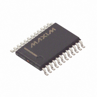
MAX5590BEUG+ Maxim Integrated Products, MAX5590BEUG+ Datasheet - Page 30

MAX5590BEUG+
Manufacturer Part Number
MAX5590BEUG+
Description
IC DAC 12BIT OCTAL BUFF 24-TSSOP
Manufacturer
Maxim Integrated Products
Datasheet
1.MAX5590BEUG.pdf
(33 pages)
Specifications of MAX5590BEUG+
Settling Time
3µs
Number Of Bits
12
Data Interface
Serial
Number Of Converters
8
Voltage Supply Source
Analog and Digital
Operating Temperature
-40°C ~ 85°C
Mounting Type
Surface Mount
Package / Case
24-TSSOP
Resolution
12 bit
Interface Type
Serial (SPI)
Supply Voltage (max)
5.25 V
Supply Voltage (min)
2.7 V
Maximum Operating Temperature
+ 85 C
Mounting Style
SMD/SMT
Minimum Operating Temperature
- 40 C
Supply Current
3.2 mA
Voltage Reference
External
Lead Free Status / RoHS Status
Lead free / RoHS Compliant
Power Dissipation (max)
-
Lead Free Status / Rohs Status
Lead free / RoHS Compliant
Buffered, Fast-Settling, Octal, 12/10/8-Bit,
Voltage-Output DACs
Figure 7 shows the unity-gain MAX5590 in a unipolar
output configuration. Table 24 lists the unipolar out-
put codes.
The MAX5590 outputs can be configured for bipolar
operation, as shown in Figure 8. The output voltage is
given by the following equation:
where CODE represents the numeric value of the
DAC’s binary input code (0 to 4095 decimal). Table 25
shows digital codes and the corresponding output volt-
age for the Figure 8 circuit.
The MAX5591/MAX5593/MAX5595 have force-sense
outputs, which provide a direct connection to the invert-
ing terminal of the output op amp, yielding the most
flexibility. The force-sense output has the advantage
that specific gains can be set externally for a given
application. The gain error for the MAX5591/MAX5593/
MAX5595 is specified in a unity-gain configuration (op-
amp output and inverting terminals connected), and
additional gain error results from external resistor
tolerances. The force-sense DACs allow many useful
circuits to be created with only a few simple external
components.
An example of a custom, fixed gain using the
MAX5591’s force-sense output is shown in Figure 9. In
this example, the external reference is set to 1.25V, and
the gain is set to +1.1V/V with external discrete resis-
tors to provide an approximate 0 to 1.375V DAC output
voltage range.
where CODE represents the numeric value of the
DAC’s binary input code (0 to 4095 decimal).
In this example, R2 = 12kΩ and R1 = 10kΩ to set the
gain = 1.1V/V.
30
V
OUT
______________________________________________________________________________________
V
= [(0.5 x V
OUT
V
OUT_
= [(0.5 x 1.25V x CODE) / 4096] x 2.2
Applications Information
= V
REF_
REF
x CODE) / 4096] x [1 + (R2 / R1)]
Configurable Output Gain
x (CODE - 2048) / 2048
Unipolar Output
Bipolar Output
Figure 8. Bipolar Output Circuit
Figure 9. Configurable Output Gain
Table 25. Bipolar Code Table (Gain = +1)
MSB
1111
1000
1000
0111
0000
0000
REF
REF
DAC CONTENTS
MAX5590
DAC_
1111
0000
0000
1111
0000
0000
MAX5591
DAC_
1111
0001
0000
1111
0001
0000
LSB
-V
10kΩ
REF
+V
ANALOG OUTPUT
-V
+V
-V
REF
(2048 / 2048) = -V
OUT_
REF
REF
REF
(2047 / 2048)
OUT_
FB_
(2047 / 2048)
10kΩ
(1 / 2048)
(1 / 2048)
0
V+
V-
R2 = 12kΩ
0.1%
25ppm
R1 = 10kΩ
0.1%
25ppm
REF
V
OUT


