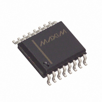
MAX536BCWE+ Maxim Integrated Products, MAX536BCWE+ Datasheet - Page 2

MAX536BCWE+
Manufacturer Part Number
MAX536BCWE+
Description
IC DAC QUAD CALBRTD 12BIT 16SOIC
Manufacturer
Maxim Integrated Products
Datasheet
1.MAX536BCWE.pdf
(24 pages)
Specifications of MAX536BCWE+
Settling Time
3µs
Number Of Bits
12
Data Interface
Serial
Number Of Converters
4
Voltage Supply Source
Dual ±
Power Dissipation (max)
762mW
Operating Temperature
0°C ~ 70°C
Mounting Type
Surface Mount
Package / Case
16-SOIC (0.300", 7.5mm Width)
Resolution
12 bit
Interface Type
Serial (3-Wire, 4-Wire, SPI, QSPI, Microwire)
Maximum Operating Temperature
+ 70 C
Mounting Style
SMD/SMT
Minimum Operating Temperature
0 C
Lead Free Status / RoHS Status
Lead free / RoHS Compliant
V
V
SDI, SCK , CS, LDAC, TP, SDO
REFAB, REFCD to AGND or DGND .............-0.3V, (V DD + 0.3V)
OUT_ to AGND or DGND .............................................V DD , V SS
Maximum Current into Any Pin............................................50mA
ELECTRICAL CHARACTERISTICS—MAX536
(V
otherwise noted. Typical values are at T
Calibrated, Quad, 12-Bit
Voltage-Output DACs with Serial Interface
ABSOLUTE MAXIMUM RATINGS
Stresses beyond those listed under “Absolute Maximum Ratings” may cause permanent damage to the device. These are stress ratings only, and functional
operation of the device at these or any other conditions beyond those indicated in the operational sections of the specifications is not implied. Exposure to
absolute maximum rating conditions for extended periods may affect device reliability.
2
Total Unadjusted Error
(Note 1)
Offset Error
DD
SS
STATIC PERFORMANCE—ANALOG SECTION
Resolution
Integral Nonlinearity
Differential Nonlinearity
Gain Error
V
Rejection Ratio
V
Rejection Ratio
MAX536 ..................................................................-0.3V, +17V
MAX537 ....................................................................-0.3V, +7V
to AGND or DGND.....................................-0.3V, (V DD + 0.3V)
DD
DD
SS
to AGND or DGND ...............................................-7V, +0.3V
_______________________________________________________________________________________
to AGND or DGND
= +15V, V
Power-Supply
Power-Supply
PARAMETER
SS
= -5V, REFAB/REFCD = 10V, AGND = DGND = 0V, R
SYMBOL
PSRR
PSRR
TUE
DNL
INL
N
A
T
T
T
T
= +25°C.)
MAX536A
MAX536B
Guaranteed monotonic
R
R
T
T
A
A
A
A
A
A
L
L
= +25°C
= T
= +25°C
= T
=
= 5kΩ
= +25°C, 10.8V < V
= +25°C, -5.5V < V
MIN
MIN
to T
to T
MAX
MAX
CONDITIONS
SS
DD
< -4.5V
< 16.5V
Continuous Power Dissipation (T
Operating Temperature Ranges
Storage Temperature Range .............................-65°C to +150°C
Lead Temperature (soldering, 10sec) .............................+300°C
Plastic DIP (derate 10.53mW/°C above +70°C) .................842mW
Wide SO (derate 9.52mW/°C above +70°C).................762mW
Ceramic SB (derate 10.53mW/°C above +70°C)..................842mW
MAX53_AC_E/BC_E.............................................0°C to +70°C
MAX53_AE_E/BE_E ..........................................-40°C to +85°C
MAX53_AMDE/BMDE .....................................-55°C to +125°C
L
MAX536A
MAX536B
MAX536AC
MAX536BC
MAX536AE
MAX536BE
MAX536AM
MAX536BM
MAX536A
MAX536B
MAX536AC
MAX536BC
MAX536AE
MAX536BE
MAX536AM
MAX536BM
MAX536_C/E
MAX536_M
= 5k
, C
L
= 100pF, T
A
= T
MIN
12
MIN
A
= +70°C)
to T
±0.15
±0.02 ±0.125
±0.03
TYP
-0.1
-0.6
MAX
, unless
±10.0
±0.50
±0.30
±1.0
±2.0
±2.0
±3.0
±2.5
±3.5
±3.0
±4.0
±2.5
±5.0
±5.0
±7.5
±6.1
±8.5
±7.5
±1.0
±1.5
±2.0
MAX
±1
±1
UNITS
LSB/V
LSB/V
LSB
LSB
LSB
LSB
Bits
mV


