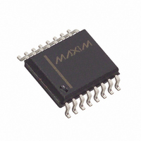
MAX536BCWE+ Maxim Integrated Products, MAX536BCWE+ Datasheet - Page 4

MAX536BCWE+
Manufacturer Part Number
MAX536BCWE+
Description
IC DAC QUAD CALBRTD 12BIT 16SOIC
Manufacturer
Maxim Integrated Products
Datasheet
1.MAX536BCWE.pdf
(24 pages)
Specifications of MAX536BCWE+
Settling Time
3µs
Number Of Bits
12
Data Interface
Serial
Number Of Converters
4
Voltage Supply Source
Dual ±
Power Dissipation (max)
762mW
Operating Temperature
0°C ~ 70°C
Mounting Type
Surface Mount
Package / Case
16-SOIC (0.300", 7.5mm Width)
Resolution
12 bit
Interface Type
Serial (3-Wire, 4-Wire, SPI, QSPI, Microwire)
Maximum Operating Temperature
+ 70 C
Mounting Style
SMD/SMT
Minimum Operating Temperature
0 C
Lead Free Status / RoHS Status
Lead free / RoHS Compliant
ELECTRICAL CHARACTERISTICS—MAX536 (continued)
(V
otherwise noted. Typical values are at T
Note 1: TUE is specified with no resistive load.
Note 2: Guaranteed by design.
Note 3: Crosstalk is defined as the glitch energy at any DAC output in response to a full-scale step change on any other DAC .
Note 4: Digital inputs at 2.4V; with digital inputs at CMOS levels, I
Note 5: All input signals are specified with t
Note 6: Serial data clocked out of SDO on SCK’s falling edge. (SDO is an open-drain output for the MAX536. The MAX537’s SDO
Note 7: Serial data clocked out of SDO on SCK’s rising edge.
Note 8: SDO changes from High-Z state to 90% of final value.
Note 9: SDO rises 10% toward High-Z state.
Calibrated, Quad, 12-Bit
Voltage-Output DACs with Serial Interface
4
TIMING CHARACTERISTICS (Note 5)
Internal Power-On Reset
Pulse Width (Note 2)
SCK Clock Period
SCK Pulse Width High
SCK Pulse Width Low
CS Fall to SCK Rise
Setup Time
SCK Rise to CS Rise
Hold Time
SDI Setup Time
SDI Hold Time
SCK Rise to SDO Valid
Propagation Delay (Note 6)
SCK Fall to SDO Valid
Propagation Delay (Note 7)
CS Fall to SDO Enable
(Note 8)
CS Rise to SDO Disable
(Note 9)
SCK Rise to CS Fall Delay
CS Rise to SCK Rise
Hold Time
LDAC Pulse Width Low
CS Pulse Width High
DD
_______________________________________________________________________________________
= +15V, V
PARAMETER
pin has an internal active pull-up.)
SS
= -5V, REFAB/REFCD = 10V, AGND = DGND = 0V, R
SYMBOL
t
t
t
t
t
t
t
LDAC
t
t
CSW
POR
t
CSH
t
DO1
DO2
t
t
CSS
t
t
CS0
CS1
t
CH
DH
CP
CL
DS
DV
TR
A
= +25°C.)
1k pull-up on SDO
to V
1k pull-up on SDO
to V
Continuous SCK, SCK edge ignored
SCK edge ignored
R
DD,
DD,
= t
F
C
C
≤ 5ns. Logic input swing is 0V to 5V.
LOAD
L OAD
= 50pF
= 50pF
CONDITIONS
DD
decreases slightly.
L
SDO high
SDO low
SDO high
SDO low
= 5k , C
L
= 100pF, T
A
= T
MIN
100
30
30
20
10
40
20
20
30
40
0
MIN
to T
TYP
MAX
26
78
50
81
53
27
40
, unless
MAX
105
110
20
80
85
45
60
UNITS
ns
ns
ns
ns
ns
ns
ns
ns
ns
ns
ns
ns
ns
ns
ns
s


