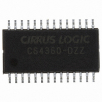
CS4360-DZZ Cirrus Logic Inc, CS4360-DZZ Datasheet - Page 3
CS4360-DZZ
Manufacturer Part Number
CS4360-DZZ
Description
IC DAC STER 6CH 102DB 28TSSOP
Manufacturer
Cirrus Logic Inc
Datasheet
1.CS4360-KZZ.pdf
(37 pages)
Specifications of CS4360-DZZ
Data Interface
Serial
Number Of Bits
24
Number Of Converters
6
Voltage Supply Source
Analog and Digital
Power Dissipation (max)
265mW
Operating Temperature
-40°C ~ 85°C
Mounting Type
Surface Mount
Package / Case
28-TSSOP
Resolution (bits)
24bit
Sampling Rate
192kSPS
Input Channel Type
Serial
Supply Current
25mA
Digital Ic Case Style
TSSOP
No. Of Pins
28
Lead Free Status / RoHS Status
Lead free / RoHS Compliant
Settling Time
-
Lead Free Status / RoHS Status
Lead free / RoHS Compliant, Lead free / RoHS Compliant
Other names
598-1056-5
Available stocks
Company
Part Number
Manufacturer
Quantity
Price
Company:

Part Number:
CS4360-DZZ
Manufacturer:
Cirrus Logic Inc
Quantity:
135
Company:
Part Number:
CS4360-DZZR
Manufacturer:
CIRRUS
Quantity:
4 000


DS517F2
5. REGISTER QUICK REFERENCE ......................................................................................... 29
6. REGISTER DESCRIPTIONS .................................................................................................. 30
7. PARAMETER DEFINITIONS .................................................................................................. 36
4.6 Popguard
4.7 Mute Control .................................................................................................................... 25
4.8 Grounding and Power Supply Arrangements .................................................................. 25
4.9 Control Port Interface ...................................................................................................... 25
6.1 Mode Control 1 (address 01h) ......................................................................................... 30
6.2 Invert Signal (address 02h) ............................................................................................. 31
6.3 Mixing Control Pair 1 (Channels A1 & B1) (address 03h)
6.4 Volume Control (addresses 06h - 0Bh) ........................................................................... 33
6.5 Mode Control 2 (address 0Dh) ......................................................................................... 33
6.6 Revision Register (Read Only) (address 0Dh) ................................................................ 35
Total Harmonic Distortion + Noise (THD+N) .......................................................................... 36
Dynamic Range ...................................................................................................................... 36
Interchannel Isolation ............................................................................................................. 36
Interchannel Gain Mismatch ................................................................................................... 36
Gain Error ............................................................................................................................... 36
Gain Drift ................................................................................................................................ 36
6.1.1 Auto-mute (AMUTE) Bit 7 ....................................................................................... 30
6.1.2 Digital Interface Format (DIF) Bit 4-6 ...................................................................... 30
6.1.3 De-emphasis Control (DEM) Bit 2-3........................................................................ 31
6.1.4 Functional Mode (FM) Bit 0-1.................................................................................. 31
6.2.1 Invert Signal Polarity (INV_xx) Bit 0-5 ..................................................................... 31
6.3.1 ATAPI Channel Mixing and Muting (atapi) Bit 0-3................................................... 32
6.4.1 MUTE (MUTE) Bit 7 ................................................................................................ 33
6.4.2 VOLUME CONTROL (xx_VOL) Bit 0-6 ................................................................... 33
6.5.1 Soft Ramp and Zero Cross CONTROL (SZC) Bit 6-7 ............................................. 33
6.5.2 Control Port Enable (CPEN) Bit 5 ........................................................................... 34
6.5.3 Power Down (PDN) Bit 4......................................................................................... 34
6.5.4 Popguard® Transient Control (POPG) Bit 3 ........................................................... 34
6.5.5 Freeze Controls (FREEZE) Bit 2............................................................................. 35
6.5.6 Master Clock DIVIDE ENABLE (MCLKDIV) Bit 1 ................................................... 35
6.5.7 Single Volume Control (SNGLVOL) Bit 0 ................................................................ 35
6.6.1 Revision Indicator (REV) [Read Only] Bit 0-3 ......................................................... 35
4.5.1 Stand-alone Mode ............................................................................................... 24
4.5.2 Control Port Mode ............................................................................................... 24
4.6.1 Power-up ............................................................................................................. 24
4.6.2 Power-down ........................................................................................................ 24
4.6.3 Discharge Time ................................................................................................... 25
4.8.1 Capacitor Placement ........................................................................................... 25
4.8.2 Power Supply Sections ....................................................................................... 25
4.9.1 Memory Address Pointer (MAP) ......................................................................... 26
4.9.2 I²C Mode ............................................................................................................. 26
4.9.3 SPI Mode ............................................................................................................ 27
Mixing Control Pair 2 (Channels A2 & B2) (address 04h)
Mixing Control Pair 3 (Channels A3 & B3) (address 05h)............................................. 31
®
4.9.1a INCR (Auto Map Increment) ................................................................ 26
4.9.1b MAP0-3 (Memory Address Pointer) ..................................................... 26
4.9.2a I²C Write ............................................................................................... 26
4.9.2b I²C Read ............................................................................................... 27
4.9.3a SPI Write .............................................................................................. 28
Transient Control .......................................................................................... 24
CS4360
3
Related parts for CS4360-DZZ
Image
Part Number
Description
Manufacturer
Datasheet
Request
R

Part Number:
Description:
IC DAC STER 6CH 102DB 28TSSOP
Manufacturer:
Cirrus Logic Inc
Datasheet:
Part Number:
Description:
IC DAC STER 6CH 102DB 28-TSSOP
Manufacturer:
Cirrus Logic Inc
Datasheet:

Part Number:
Description:
IC DAC STER 6CH 102DB 28-TSSOP
Manufacturer:
Cirrus Logic Inc
Datasheet:

Part Number:
Description:
D/A Converter (D-A) IC
Manufacturer:
Cirrus Logic Inc
Datasheet:
Part Number:
Description:
D/A Converter (D-A) IC
Manufacturer:
Cirrus Logic Inc
Datasheet:
Part Number:
Description:
Development Kit
Manufacturer:
Cirrus Logic Inc
Datasheet:
Part Number:
Description:
Development Kit
Manufacturer:
Cirrus Logic Inc
Datasheet:


Part Number:
Description:
High-efficiency PFC + Fluorescent Lamp Driver Reference Design
Manufacturer:
Cirrus Logic Inc
Datasheet:
Part Number:
Description:
Development Kit
Manufacturer:
Cirrus Logic Inc
Datasheet:
Part Number:
Description:
Development Kit
Manufacturer:
Cirrus Logic Inc
Datasheet:

Part Number:
Description:
Development Kit
Manufacturer:
Cirrus Logic Inc
Datasheet:
Part Number:
Description:
Development Kit
Manufacturer:
Cirrus Logic Inc
Datasheet:
Part Number:
Description:
Development Kit
Manufacturer:
Cirrus Logic Inc
Datasheet:

Part Number:
Description:
Ref Bd For Speakerbar MSA & DSP Products
Manufacturer:
Cirrus Logic Inc