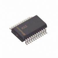
MAX5187BEEG+ Maxim Integrated Products, MAX5187BEEG+ Datasheet

MAX5187BEEG+
Specifications of MAX5187BEEG+
Related parts for MAX5187BEEG+
MAX5187BEEG+ Summary of contents
Page 1
... MAX5181/MAX5184 data sheet. Signal Reconstruction Digital Signal Processing Arbitrary Waveform Generation (AWG) Imaging Applications ________________________________________________________________ Maxim Integrated Products For pricing, delivery, and ordering information, please contact Maxim/Dallas Direct! at 1-888-629-4642, or visit Maxim’s website at www.maxim-ic.com. o +2.7V to +3.3V Single-Supply Operation o Wide Spurious-Free Dynamic Range: ...
Page 2
Current/Voltage-Output DACs ABSOLUTE MAXIMUM RATINGS AGND, DGND .................................-0. Digital Input to DGND...............................................-0.3V to +6V OUTP, OUTN, CREF to AGND .................................-0. AGND ..........................................................-0.3V to +6V REF AGND ...
Page 3
Current/Voltage-Output DACs ELECTRICAL CHARACTERISTICS (continued) ( +3V ±10%, AGND = DGND = unless otherwise noted. Typical values are at T PARAMETER SYMBOL REFERENCE Output Voltage Range V Output Voltage Temperature TCV ...
Page 4
Current/Voltage-Output DACs ( +3V, AGND = DGND = 0, 400Ω differential output INTEGRAL NONLINEARITY vs. INPUT CODE 0.150 0.125 0.100 0.075 0.050 0.025 0 -0.025 -0.050 128 160 ...
Page 5
Current/Voltage-Output DACs ( +3V, AGND = DGND = 0, 400Ω differential output SHUTDOWN CURRENT vs. TEMPERATURE 0.13 0.11 0.09 MAX5190 0.07 MAX5187 0.05 0.03 -40 - TEMPERATURE (°C) OUTPUT ...
Page 6
Current/Voltage-Output DACs ( +3V, AGND = DGND = 0, 400Ω differential output SPURIOUS-FREE DYNAMIC RANGE vs. CLOCK FREQUENCY 100 ...
Page 7
Current/Voltage-Output DACs PIN NAME 1 CREF Reference Bias Bypass 2 OUTP Positive Analog Output. Current output for MAX5187; voltage output for MAX5190. 3 OUTN Negative Analog Output. Current output for MAX5187; voltage output for MAX5190. 4 AGND Analog ...
Page 8
Current/Voltage-Output DACs 1.2V REF REFO REFR 9.6k* CLK *INTERNAL 400Ω AND 9.6kΩ RESISTORS FOR MAX5190 ONLY. Figure 1. Functional Diagram Detailed Description The MAX5187/MAX5190 are 8-bit DACs capable of operating with clock speeds up to 40MHz. Each con- ...
Page 9
Current/Voltage-Output DACs OPTIONAL EXTERNAL BUFFER FOR HEAVIER LOADS MAX4040 AGND V REF I = REF R SET *COMPENSATION CAPACITOR (C = 100nF) COMP Figure 2. Setting I with the Internal +1.2V Reference and the Control Amplifier FS AV ...
Page 10
Current/Voltage-Output DACs External Reference To disable the MAX5187/MAX5190’s internal reference, connect REN temperature-stable external ref- DD erence may now be applied to drive the REFO pin to set the full-scale output (Figure 3). Choose ...
Page 11
Current/Voltage-Output DACs The MAX5187 output is designed to supply full-scale output currents of 1mA into 400Ω loads in parallel with a capacitive load of 5pF. The MAX5190 features inte- grated 400Ω resistors that restore the array current to ...
Page 12
Current/Voltage-Output DACs +3V +3V 10µF 0.1µF AV CLK D0–D7 REFO 0.1µF REFR R ** SET *400Ω RESISTORS INTERNAL TO MAX5190 ONLY. **MAX5187 ONLY Figure 6. Differential to Single-Ended Conversion Using a Low-Distortion Amplifier Gain error (Figure 5d) is ...
Page 13
Current/Voltage-Output DACs +3V 8 DIGITAL SIGNAL PROCESSOR 8 Figure 7. Using the MAX5187/MAX5190 for I/Q Signal Reconstruction In a typical QAM application (Figure 7), the modulation occurs in the digital domain, and two DACs such as the MAX5187/MAX5190 ...
Page 14
Current/Voltage-Output DACs COUNTER ADR CLOCK GENERATOR *MAX5187 ONLY Figure 8a. Traditional Arbitrary Waveform Generation (AWG) CLOCK GENERATOR A D PHASE D PIR ACCUMULATOR E R PHASE INCREMENT ACCUMULATOR REGISTER FEEDBACK LOOP FOR DATA BITS *MAX5187 ONLY Figure 8b. ...
Page 15
... Maxim cannot assume responsibility for use of any circuitry other than circuitry entirely embodied in a Maxim product. No circuit patent licenses are implied. Maxim reserves the right to change the circuitry and specifications without notice at any time. Maxim Integrated Products, 120 San Gabriel Drive, Sunnyvale, CA 94086 408-737-7600 ____________________ 15 © 2001 Maxim Integrated Products Printed USA is a registered trademark of Maxim Integrated Products ...


