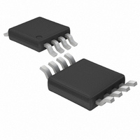
LTC1669-8CMS8 Linear Technology, LTC1669-8CMS8 Datasheet - Page 11

LTC1669-8CMS8
Manufacturer Part Number
LTC1669-8CMS8
Description
IC DAC 10-BIT V-OUT I2C 8-MSOP
Manufacturer
Linear Technology
Datasheet
1.LTC1669CMS8PBF.pdf
(16 pages)
Specifications of LTC1669-8CMS8
Settling Time
30µs
Number Of Bits
10
Data Interface
I²C
Number Of Converters
1
Voltage Supply Source
Single Supply
Power Dissipation (max)
630µW
Operating Temperature
0°C ~ 70°C
Mounting Type
Surface Mount
Package / Case
8-MSOP, Micro8™, 8-uMAX, 8-uSOP,
Lead Free Status / RoHS Status
Contains lead / RoHS non-compliant
Available stocks
Company
Part Number
Manufacturer
Quantity
Price
Company:
Part Number:
LTC1669-8CMS8
Manufacturer:
LT
Quantity:
10 000
Company:
Part Number:
LTC1669-8CMS8#TRPBF
Manufacturer:
LINEAR
Quantity:
8 196
APPLICATIONS INFORMATION
SYNC Address/Quick Command
In addition to the slave address, the LTC1669 has an address
that can be shared by other devices so that they may be
updated synchronously. The address is called to the SYNC
address and uses the quick command protocol.
The SYNC Address is 1111 110
The SY/CLR bit set high only has meaning when the “SY”
bit of the command byte was previously set HIGH. On
the otherhand, the SY/CLR bit set LOW will always clear
the part, independent of the state of the “SY” bit in the
command byte.
Voltage Output
The output amplifi er contained in the LTC1669 can source
or sink up to 5mA. The output stage swings to within a
few millivolts of either supply rail when unloaded and
has an equivalent output resistance of 85Ω when driving
a load to the rails. The output amplifi er is stable driving
capacitive loads up to 1000pF .
A small resistor placed in series with the output can be
used to achieve stability for any load capacitance greater
than 1000pF . For example, a 0.1μF load can be driven
by the LTC1669 if a 110Ω series resistance is used. The
phase margin of the resulting circuit is 45° and increases
monotonically from this point if larger values of resistance,
capacitance or both are substituted for the values given.
SY/CLR
1
0
Start
1
Update output latches on rising edge of SCL during
Acknowledge of SYNC Address
Clear all internal latches on rising edge of SCL during
Acknowledge of SYNC Address
SYNC Address
1111 110
7
SY/CLR
1
Ack
1
Stop
1669 TA05
1
Rail-to-Rail Output Considerations
As in any rail-to-rail device, the output is limited to volt-
ages within the supply range.
If the DAC offset is negative, the output for the lowest
codes limits at 0V as shown in Figure 1b.
Similarly, limiting can occur near full scale when V
used as the reference. If V
error (FSE) is positive, the output for the highest codes
limits at V
can occur if the internal reference is used.
Offset and linearity are defi ned and tested over the region
of the DAC transfer function where no output limiting can
occur.
Internal Reference
In applications where a predictable output is required
that is independent of supply voltage, the LTC1669 has a
user-selectable internal reference. Selecting the internal
reference will set the full-scale output voltage to 2.5V. This
can be useful in applications where the supply voltage is
poorly regulated.
Using the LT
Power Supply for the LTC1669
In applications where the advantages of using the internal
reference are required but the full-scale range needs to
be greater than 2.5V, an external series reference can be
used. The LT1460 is ideal for use as a power supply for
the LTC1669 and can provide 3V, 3.3V and 5V full-scale
output voltage ranges. The LT1460 provides accuracy, noise
immunity and extended supply range to the LTC1669 when
the LTC1669 is operated ratiometric to V
parts are available in SOT-23 packages, the PC board space
for this application is extremely small. See Figure 2.
CC
®
as shown in Figure 1c. No full-scale limiting
1460 Micropower Series Reference as a
REF
= V
CC
and the DAC full-scale
LTC1669
CC
. Since both
11
CC
1669fa
is


