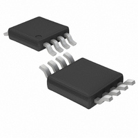
LTC1669-8CMS8 Linear Technology, LTC1669-8CMS8 Datasheet - Page 7

LTC1669-8CMS8
Manufacturer Part Number
LTC1669-8CMS8
Description
IC DAC 10-BIT V-OUT I2C 8-MSOP
Manufacturer
Linear Technology
Datasheet
1.LTC1669CMS8PBF.pdf
(16 pages)
Specifications of LTC1669-8CMS8
Settling Time
30µs
Number Of Bits
10
Data Interface
I²C
Number Of Converters
1
Voltage Supply Source
Single Supply
Power Dissipation (max)
630µW
Operating Temperature
0°C ~ 70°C
Mounting Type
Surface Mount
Package / Case
8-MSOP, Micro8™, 8-uMAX, 8-uSOP,
Lead Free Status / RoHS Status
Contains lead / RoHS non-compliant
Available stocks
Company
Part Number
Manufacturer
Quantity
Price
Company:
Part Number:
LTC1669-8CMS8
Manufacturer:
LT
Quantity:
10 000
Company:
Part Number:
LTC1669-8CMS8#TRPBF
Manufacturer:
LINEAR
Quantity:
8 196
DEFINITIONS
Differential Nonlinearity (DNL): The difference between
the measured change and the ideal 1LSB change for any
two adjacent codes. The DNL error between any two codes
is calculated as follows:
Where ΔV
two adjacent codes.
Digital Feedthrough: The glitch that appears at the ana-
log output caused by AC coupling from the digital inputs
when they change state. The area of the glitch is specifi ed
in (nV)(sec).
Full-Scale Error (FSE): The deviation of the actual full-scale
voltage from ideal. FSE includes the effects of offset and
gain errors (see Applications Information).
Integral Nonlinearity (INL): The deviation from a straight
line passing through the endpoints of the DAC transfer
curve (Endpoint INL). Because the output cannot go
below zero, the linearity is measured between full scale
and the lowest code that guarantees the output will be
DNL = (ΔV
OUT
OUT
is the measured voltage difference between
– LSB)/LSB
greater than zero. The INL error at a given input code is
calculated as follows:
Where V
at the given input code.
Least Signifi cant Bit (LSB): The ideal voltage difference
between two successive codes.
Resolution (n): Defi nes the number of DAC output states
(2
imply linearity.
Voltage Offset Error (V
output when the DAC is loaded with all zeros. A single
supply DAC can have a true negative offset, but the output
cannot go below zero (see Applications Information).
For this reason, single supply DAC offset is measured at
the lowest code that guarantees the output will be greater
than zero.
n
INL = [V
LSB = V
) that divide the full-scale range. Resolution does not
OUT
REF
OUT
is the output voltage of the DAC measured
/1024
– V
OS
– (V
OS
): Nominally, the voltage at the
FS
– V
OS
)(code/1023)]/LSB
LTC1669
1669fa
7


