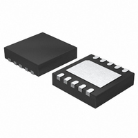
LTC2611CDD Linear Technology, LTC2611CDD Datasheet - Page 3

LTC2611CDD
Manufacturer Part Number
LTC2611CDD
Description
IC DAC 14BIT SGL R-R VOUT 10DFN
Manufacturer
Linear Technology
Datasheet
1.LTC2621CDDPBF.pdf
(16 pages)
Specifications of LTC2611CDD
Settling Time
9µs
Number Of Bits
14
Data Interface
Serial
Number Of Converters
1
Voltage Supply Source
Single Supply
Power Dissipation (max)
1.88mW
Operating Temperature
0°C ~ 70°C
Mounting Type
Surface Mount
Package / Case
10-DFN
Lead Free Status / RoHS Status
Contains lead / RoHS non-compliant
Available stocks
Company
Part Number
Manufacturer
Quantity
Price
Company:
Part Number:
LTC2611CDD
Manufacturer:
LT
Quantity:
10 000
Part Number:
LTC2611CDD
Manufacturer:
LTNEAR
Quantity:
20 000
Company:
Part Number:
LTC2611CDD-1
Manufacturer:
LT
Quantity:
10 000
Company:
Part Number:
LTC2611CDD-1#PBF
Manufacturer:
Linear Technology
Quantity:
135
ELECTRICAL CHARACTERISTICS
temperature range, otherwise specifi cations are at T
unless otherwise noted.
SYMBOL PARAMETER
DC Performance
DNL
INL
ZSE
V
GE
The
REF = 4.096V (V
SYMBOL PARAMETER
PSR
R
I
Reference Input
I
Power Supply
V
I
Digital I/O
V
SC
REF
CC
OS
CC
IH
OUT
l
denotes the specifi cations which apply over the full operating temperature range, otherwise specifi cations are at T
Resolution
Monotonicity
Differential Nonlinearity (Note 2)
Integral Nonlinearity
Load Regulation
Zero-Scale Error
Offset Error
V
Coeffi cient
Gain Error
Gain Temperature
Coeffi cient
Power Supply Rejection
DC Output Impedance
Short-Circuit Output Current
Input Voltage Range
Resistance
Capacitance
Reference Current, Power Down Mode DAC Powered Down
Positive Supply Voltage
Supply Current
Digital Input High Voltage
OS
Temperature
CC
= 5V), REF = 2.048V (V
CONDITIONS
(Note 2)
(Note 2)
V
V
Code = 0
(Note 5)
REF
REF
I
I
I
I
OUT
OUT
OUT
OUT
= V
= V
= 0mA to 15mA Sourcing
= 0mA to 15mA Sinking
= 0mA to 7.5mA Sourcing
= 0mA to 7.5mA Sinking
CC
CC
= 5V, Midscale
= 2.5V, Midscale
CC
CONDITIONS
V
V
V
V
V
V
Normal Mode
For Specifi ed Performance
V
V
DAC Powered Down (Note 3) V
DAC Powered Down (Note 3) V
V
V
= 2.5V), V
CC
CC
REF
REF
CC
CC
CC
CC
CC
CC
Code: Zero Scale; Forcing Output to V
Code: Full Scale; Forcing Output to GND
Code: Zero Scale; Forcing Output to V
Code: Full Scale; Forcing Output to GND
= 5V ±10%
= 3V ±10%
= 5.5V, V
= 2.5V, V
= 5V (Note 3)
= 3V (Note 3)
= 2.5V to 5.5V
= 2.5V to 3.6V
= V
= V
CC
CC
A
= 25°C. REF = 4.096V (V
= 5V, Midscale; –15mA ≤ I
= 2.5V, Midscale; –7.5mA ≤ I
OUT
REF
REF
The
unloaded, unless otherwise noted. (Note 8)
= 5.5V
= 2.5V
l
l
l
l
l
l
l
l
l
l
l
l
denotes the specifi cations which apply over the full operating
LTC2621/ LTC2621-1 LTC2611/ LTC2611-1 LTC2601/ LTC2601-1
MIN
12
12
LTC2601/LTC2611/LTC2621
CC
CC
±0.03 ±0.7
±0.8
0.03
0.04
0.06
0.08
±1.5
TYP
= 5V
= 3V
±5
±2
1
OUT
CC
OUT
0.125
0.125
MAX
CC
CC
±0.5
0.25
0.25
≤ 15mA
= 5V), REF = 2.048V (V
±4
±9
9
≤ 7.5mA
MIN
14
14
l
l
l
l
l
l
l
l
l
l
l
l
l
l
l
l
l
0.10
0.15
±1.5
±0.1
TYP
0.2
0.3
±3
±5
±2
1
MIN
7.5
7.5
2.5
2.4
2.0
15
15
88
0
MAX
±0.7
±16
0.5
0.5
±1
±9
1
1
9
CC
= 2.5V), V
MIN
0.001
0.375
16
16
0.04
0.05
0.30
0.40
0.10
TYP
–80
–80
124
35
39
20
27
15
±0.05 ±0.7
0.45
0.60
±1.5
TYP
±13
0.9
1.2
±5
±2
1
OUT
MAX
0.15
0.15
VCC
0.55
0.45
160
5.5
60
60
50
50
1
1
1
A
unloaded,
MAX
±64
±1
±9
= 25°C.
2
2
4
4
9
LSB/mA
LSB/mA
LSB/mA
LSB/mA
ppm/°C
UNITS
UNITS
%FSR
μV/°C
2601fb
3
LSB
LSB
Bits
Bits
mV
mV
mA
mA
mA
mA
mA
mA
kΩ
dB
dB
μA
μA
μA
pF
Ω
Ω
V
V
V
V


