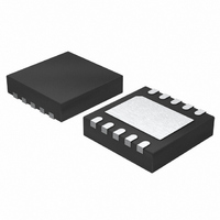
LTC2611CDD Linear Technology, LTC2611CDD Datasheet

LTC2611CDD
Specifications of LTC2611CDD
Available stocks
Related parts for LTC2611CDD
LTC2611CDD Summary of contents
Page 1
... The power-on reset circuit resets the LTC2601-1/LTC2611-1/LTC2621-1 to midscale. The volt- age outputs stay at midscale until a valid write and update take place. L, LT, LTC and LTM are registered trademarks of Linear Technology Corporation. All other trademarks are the property of their respective owners. Protected by U.S. Patents including 5396245. 6 ...
Page 2
... LTC2601CDD-1#TRPBF LTC2601IDD-1#PBF LTC2601IDD-1#TRPBF LTC2611CDD-1#PBF LTC2611CDD-1#TRPBF LTC2611IDD-1#PBF LTC2611IDD-1#TRPBF LTC2621CDD-1#PBF LTC2621CDD-1#TRPBF LTC2621IDD-1#PBF LTC2621IDD-1#TRPBF LEAD BASED FINISH TAPE AND REEL LTC2601CDD LTC2601CDD#TR LTC2601IDD LTC2601IDD#TR LTC2611CDD LTC2611CDD#TR LTC2611IDD LTC2611IDD#TR LTC2621CDD LTC2621CDD#TR LTC2621IDD LTC2621IDD#TR LTC2601CDD-1 LTC2601CDD-1#TR LTC2601IDD-1 LTC2601IDD-1#TR LTC2611CDD-1 LTC2611CDD-1#TR LTC2611IDD-1 LTC2611IDD-1#TR LTC2621CDD-1 LTC2621CDD-1#TR LTC2621IDD-1 LTC2621IDD-1#TR Consult LTC Marketing for parts specifi ...
Page 3
ELECTRICAL CHARACTERISTICS temperature range, otherwise specifi cations are at T unless otherwise noted. SYMBOL PARAMETER CONDITIONS DC Performance Resolution Monotonicity (Note 2) DNL Differential Nonlinearity (Note 2) INL Integral Nonlinearity (Note 2) Load Regulation REF CC I ...
Page 4
LTC2601/LTC2611/LTC2621 ELECTRICAL CHARACTERISTICS temperature range, otherwise specifi cations are at T unless otherwise noted. (Note 8) SYMBOL PARAMETER V Digital Input Low Voltage IL V Digital Output High Voltage OH V Digital Output Low Voltage OL I Digital Input Leakage ...
Page 5
TIMING CHARACTERISTICS Note 1: Stresses beyond those listed under Absolute Maximum Ratings may cause permanent damage to the device. Exposure to any Absolute Maximum Rating condition for extended periods may affect device reliability and lifetime. Note 2: Linearity and monotonicity ...
Page 6
LTC2601/LTC2611/LTC2621 TYPICAL PERFORMANCE CHARACTERISTICS LTC2601 Settling to ±1LSB V OUT 100μV/DIV CS/LD 2V/DIV 2μs/DIV 4.096V CC REF 1/4-SCALE TO 3/4-SCALE STEP 200pF L L AVERAGE OF 2048 EVENTS LTC2611 Integral ...
Page 7
TYPICAL PERFORMANCE CHARACTERISTICS LTC2601/LTC2611/LTC2621 Current Limiting 0.10 CODE = MIDSCALE 0. REF CC 0. REF CC 0.04 0.02 0 –0. REF CC –0. ...
Page 8
LTC2601/LTC2611/LTC2621 TYPICAL PERFORMANCE CHARACTERISTICS LTC2601/LTC2611/LTC2621 Midscale Glitch Impulse V OUT 10mV/DIV 12nV-s TYP CS/LD 5V/DIV 2601 G26 2.5μs/DIV Supply Current vs Logic Voltage 1 SWEEP SCK, SDI 1.2 AND CS/ 1.0 0.8 ...
Page 9
TYPICAL PERFORMANCE CHARACTERISTICS LTC2601/LTC2611/LTC2621 Short-Circuit Output Current vs V (Sinking) OUT 5. 5.6V REF CODE = SWEPT OUT 1V/DIV ...
Page 10
LTC2601/LTC2611/LTC2621 BLOCK DIAGRAM SDI 2 SCK 3 32-BIT SHIFT REGISTER CS/LD 5 SDO 1 TIMING DIAGRAMS SCK SDI CS/LD SDO LDAC 10 6 REF INPUT DAC REGISTER REGISTER CONTROL DECODE LOGIC LDAC CLR ...
Page 11
OPERATION Power-On Reset The LTC2601/LTC2611/LTC2621 clear the outputs to zero scale when power is fi rst applied, making system initializa- tion consistent and repeatable. The LTC2601-1/LTC2611- 1/LTC2621-1 set the voltage outputs to midscale when power is fi rst applied. For ...
Page 12
LTC2601/LTC2611/LTC2621 OPERATION INPUT WORD (LTC2601) COMMAND DON’T CARE BITS INPUT WORD (LTC2611) COMMAND DON’T CARE BITS INPUT WORD (LTC2621) COMMAND DON’T CARE BITS ...
Page 13
OPERATION the rising edge of CS/LD, then LDAC is recognized, the command specifi the 24-bit word just transferred is executed and the DAC output is updated. The DAC is powered up when LDAC is taken low, inde- pendent ...
Page 14
LTC2601/LTC2611/LTC2621 OPERATION 14 2601fb ...
Page 15
... SHADED AREA IS ONLY A REFERENCE FOR PIN 1 LOCATION ON THE TOP AND BOTTOM OF PACKAGE Information furnished by Linear Technology Corporation is believed to be accurate and reliable. However, no responsibility is assumed for its use. Linear Technology Corporation makes no representa- tion that the interconnection of its circuits as described herein will not infringe on existing patent rights. LTC2601/LTC2611/LTC2621 ...
Page 16
... DAC, 2.7V to 5.5V Supply Range, Rail-to-Rail 2 Output Interface 2 Output Interface 250μA Range per DAC, 2.7V to 5.5V Supply Range, Rail-to-Rail Output with Separate V Pins for Each DAC REF LT 0409 REV B • PRINTED IN USA © LINEAR TECHNOLOGY CORPORATION 2004 2601fb ...


