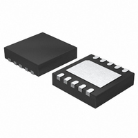
LTC2642AIDD-16#PBF Linear Technology, LTC2642AIDD-16#PBF Datasheet - Page 16

LTC2642AIDD-16#PBF
Manufacturer Part Number
LTC2642AIDD-16#PBF
Description
IC DAC 16BIT VOUT 10-DFN
Manufacturer
Linear Technology
Datasheet
1.LTC2642CDD-12PBF.pdf
(24 pages)
Specifications of LTC2642AIDD-16#PBF
Settling Time
1µs
Number Of Bits
16
Data Interface
Serial
Number Of Converters
1
Voltage Supply Source
Single Supply
Power Dissipation (max)
600µW
Operating Temperature
-40°C ~ 85°C
Mounting Type
Surface Mount
Package / Case
10-DFN
Lead Free Status / RoHS Status
Lead free / RoHS Compliant
Available stocks
Company
Part Number
Manufacturer
Quantity
Price
LTC2641/LTC2642
such as the LTC6078 is suitable, if the application does
not require linear operation very near to GND, or zero scale
(Figure 2). The LTC6078 typically swings to within 1mV of
GND if it is not required to sink any load current. For an
LSB size of 38μV, 1mV represents 26 missing codes near
zero scale. Linearity will be degraded over a somewhat
larger range of codes above GND. It is also unavoidable
that settling time and transient performance will degrade
whenever a single supply amplifi er is operated very close
to GND, or to the positive supply rail.
The small LSB size of a 16-bit DAC, coupled with the tight
accuracy specifi cations on the LTC2641/LTC2642, means
that the accuracy and input specifi cations for the external
op amp are critical for overall DAC performance.
Op Amp Specifi cations and Unipolar DAC Accuracy
Most op amp accuracy specifi cations convert easily to
DAC accuracy.
Op amp input bias current on the noninverting (+) input is
equivalent to an I
produces a DAC zero-scale error (ZSE) (see Unbuffered
Operation):
In 16-bit LSBs:
Op amp input impedance, R
loading the LTC2641/LTC2642 V
a gain error of:
Op amp offset voltage, V
zero code offset error, ZSE:
Temperature effects also must be considered. Over the
–40°C to 85°C industrial temperature range, an offset
APPLICATIONS INFORMATION
16
ZSE = –I
GE =
ZSE = –I
ZSE V
=
1+
–66k
OS
B
B
(IN+) • R
6.2k
( )
R
IN
•
IN
V
+
66
L
REF
loading the DAC V
• 6.2k •
k
LSB
OUT
[ ]
LSB
OS
[Volts]
, corresponds directly to DAC
V
66k
REF
IN
, is equivalent to an R
OUT
LSB
OUT
pin, and produces
pin and therefore
L
voltage temperature coeffi cient (referenced to 25°C) of
0.6μV/°C will add 1LSB of zero-scale error. Also, I
the V
relative variation over temperature.
Op amp open-loop gain, A
error (GE):
Op amp input common mode rejection ratio (CMRR) is
an input-referred error that corresponds to a combina-
tion of gain error (GE) and INL, depending on the op amp
architecture and operating conditions. A conservative
estimate of total CMRR error is:
where V
dB) is specifi ed over. Op amp Typical Performance Charac-
teristics graphs are useful to predict the impact of CMRR
errors on DAC performance. Typically, a precision op amp
will exhibit a fairly linear CMRR behavior (corresponding
to DAC gain error only) over most of the common mode
input range (CMR), and become nonlinear and produce
signifi cant errors near the edge of the CMR.
Rail-to-rail input op amps are a special case, because they
have 2 distinct input stages, one with CMR to GND and
the other with CMR to V
CM input region where operation switches between the
two input stages.
The LTC6078 rail-to-rail input op amp typically exhibits
remarkably low crossover linearity error, as shown in the
V
(see the LTC6078 data sheet). Crossover occurs at CM
inputs about 1V below V
a unipolar DAC buffer with V
typically add only about 1LSB of GE and almost no INL
error due to CMRR. Even in a full rail-to-rail application,
with V
1LSB of INL at 16-bits.
OS
GE
Error = 10
vs V
OFFSET
REF
=
CMRR_RANGE
A
CM
66
= V
VOL
error it causes, will typically show signifi cant
k
Typical Performance Characteristics graphs
+
= 5V, a typical LTC6078 will add only about
CMRR
[ ]
LSB
20
is the voltage range that CMRR (in
•
+
+
V
, and an LTC6078 operating as
. This results in a “crossover”
CMRR _RANGE
VOL
REF
V
, contributes to DAC gain
REF
= 2.5V and V
• 66k LSB
+
= 5V will
BIAS
26412fb
and


