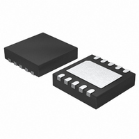
LTC2642AIDD-16#PBF Linear Technology, LTC2642AIDD-16#PBF Datasheet - Page 19

LTC2642AIDD-16#PBF
Manufacturer Part Number
LTC2642AIDD-16#PBF
Description
IC DAC 16BIT VOUT 10-DFN
Manufacturer
Linear Technology
Datasheet
1.LTC2642CDD-12PBF.pdf
(24 pages)
Specifications of LTC2642AIDD-16#PBF
Settling Time
1µs
Number Of Bits
16
Data Interface
Serial
Number Of Converters
1
Voltage Supply Source
Single Supply
Power Dissipation (max)
600µW
Operating Temperature
-40°C ~ 85°C
Mounting Type
Surface Mount
Package / Case
10-DFN
Lead Free Status / RoHS Status
Lead free / RoHS Compliant
Available stocks
Company
Part Number
Manufacturer
Quantity
Price
APPLICATIONS INFORMATION
on the digital inputs is imperceptible, thanks to the digital
input hysteresis)
Just by maintaining separate areas on the GND plane
where analog and digital return currents naturally fl ow,
good results are generally achieved. Only after this has
been done, it is sometimes useful to interrupt the ground
plane with strategically placed “slots”, to prevent the digital
ground currents from fringing into the analog portion of
the plane. When doing this, the gap in the plane should be
only as long as it needs to be to serve its purpose.
PACKAGE DESCRIPTION
3.5 ±0.05
2.15 ±0.05
RECOMMENDED SOLDER PAD PITCH AND DIMENSIONS
NOTE:
1. DRAWING TO BE MADE A JEDEC PACKAGE OUTLINE M0-229 VARIATION OF (WEED-1)
2. DRAWING NOT TO SCALE
3. ALL DIMENSIONS ARE IN MILLIMETERS
4. DIMENSIONS OF EXPOSED PAD ON BOTTOM OF PACKAGE DO NOT INCLUDE
5. EXPOSED PAD SHALL BE SOLDER PLATED
6. SHADED AREA IS ONLY A REFERENCE FOR PIN 1 LOCATION
1.65 ±0.05
(2 SIDES)
MOLD FLASH. MOLD FLASH, IF PRESENT, SHALL NOT EXCEED 0.15mm ON ANY SIDE
ON TOP AND BOTTOM OF PACKAGE
0.25 ± 0.05
2.38 ±0.05
(2 SIDES)
0.50
BSC
0.675 ±0.05
PACKAGE
OUTLINE
8-Lead Plastic DFN (3mm × 3mm)
(Reference LTC DWG # 05-08-1698)
TOP MARK
(NOTE 6)
PIN 1
DD Package
0.200 REF
Caution: if a GND plane gap is improperly placed, so that
it interrupts a signifi cant GND return path, or if a signal
traces crosses over the gap, then adding the gap may
greatly degrade performance! In this case, the GND and
signal return currents are forced to fl ow the long way
around the gap, and then are typically channeled directly
into the most sensitive area of the analog GND plane.
0.75 ±0.05
3.00 ±0.10
(4 SIDES)
LTC2641/LTC2642
0.00 – 0.05
1.65 ± 0.10
(2 SIDES)
BOTTOM VIEW—EXPOSED PAD
0.25 ± 0.05
R = 0.115
TYP
4
5
2.38 ±0.10
(2 SIDES)
8
1
0.50 BSC
19
0.38 ± 0.10
26412fb
(DD) DFN 1203


