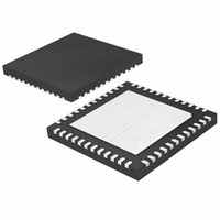
LTC2753IUK-14#PBF Linear Technology, LTC2753IUK-14#PBF Datasheet - Page 15

LTC2753IUK-14#PBF
Manufacturer Part Number
LTC2753IUK-14#PBF
Description
IC DAC 14BIT DUAL 48-QFN
Manufacturer
Linear Technology
Series
SoftSpan™r
Datasheet
1.LTC2753CUK-12PBF.pdf
(24 pages)
Specifications of LTC2753IUK-14#PBF
Settling Time
2µs
Number Of Bits
14
Data Interface
Parallel
Number Of Converters
2
Voltage Supply Source
Single Supply
Operating Temperature
-40°C ~ 85°C
Mounting Type
Surface Mount
Package / Case
48-QFN
Lead Free Status / RoHS Status
Lead free / RoHS Compliant
Power Dissipation (max)
-
OPERATION
These devices also have a power-on reset that initializes
both DACs to V
power up in the 0V-5V range if the part is in SoftSpan
confi guration; for manual span (see Manual Span Confi gu-
ration below), both DACs power up in the manually-chosen
range at the appropriate code.
Manual Span Confi guration
Multiple output ranges are not needed in some applications.
To confi gure the LTC2753 for single-span operation, tie the
MSPAN pin to V
output range is then specifi ed by the span I/O pins (S0,
S1 and S2) as usual, but the pins are programmed by ty-
ing directly to GND or V
this confi guration, both DAC channels will initialize to the
chosen output range at power-up, with V
When confi gured for manual span operation, span pin
readback is disabled.
Readback
The contents of any one of the 8 interface registers can
be read back from the I/O ports.
The I/O pins are grouped into two ports: data and span. The
data I/O port comprises pins D0-D11, D0-D13 or D0-D15
(LTC2753-12, LTC2753-14 or LTC2753-16, respectively).
The span I/O port comprises pins S0, S1 and S2 for all
parts.
Each DAC channel has a set of data registers that are
controlled and read back from the data I/O port; and a set
of span registers that are controlled and read back from
the span I/O port. The register structure is shown in the
Block Diagram.
A readback operation is initiated by asserting READ to
logic high after selecting the desired DAC channel and I/O
port. The I/O pins, which are high-impedance digital inputs
when READ is low, selectively change to low-impedance
logic outputs during readback.
Select the DAC channel with address pins A1 and A0, and
select the I/O port (data or span) to be read back with
OUT
DD
and the D/S pin to GND. The desired
= 0V in any output range. The DACs
DD
(see Figure 1 and Table 2). In
OUT
= 0V.
the D/S pin. The selected I/O port’s pins become logic
outputs during readback, while the unselected I/O port’s
pins remain high-impedance inputs.
With the DAC channel and I/O port selected, assert READ
high and select the desired input or DAC register using the
UPD pin. Note that UPD is a two function pin—the update
function is only available when READ is low. When READ
is high, the update function is disabled and the UPD pin
instead selects the input or DAC register for readback.
Table 1 shows the readback functions for the LTC2753.
Table 1. Write, Update and Read Functions
READ D/S
X = Don’t Care
The most common readback task is to check the contents
of an input register after writing to it, before updating the
new data to the DAC register. To do this, hold UPD low
and assert READ high. The contents of the selected port’s
input register are output to its I/O pins.
To read back the contents of a DAC register, hold UPD low
and assert READ high, then bring UPD high to select the
DAC register. The contents of the selected DAC register are
output by the selected port’s I/O pins. Note: if no update is
desired after the readback operation, UPD must be returned
low before bringing READ low; otherwise the UPD pin will
revert to its primary function and update the DAC.
0
0
0
0
0
0
0
0
1
1
1
1
0
0
0
0
1
1
1
1
0
0
1
1
WR UPD
0
0
1
1
0
0
1
1
X
X
X
X
0
1
0
1
0
1
0
1
0
1
0
1
Write to Input Register
Update DAC Register
Update DAC register
Read Input Register
Read DAC Register
(Transparent)
Write/Update
SPAN I/O
-
-
-
-
-
-
Write to Input Register
LTC2753
Update DAC Register
Update DAC Register
Read Input Register
Read DAC Register
Write/Update
(Transparent)
DATA I/O
-
-
-
-
-
-
15
2753f


