LTC2753IUK-12#TRPBF Linear Technology, LTC2753IUK-12#TRPBF Datasheet
LTC2753IUK-12#TRPBF
Specifications of LTC2753IUK-12#TRPBF


Related parts for LTC2753IUK-12#TRPBF


LTC2753IUK-12#TRPBF Summary of contents
Page 1
... DACs any output range. The parts are specifi ed over commercial and industrial temperature ranges LTC and LTM are registered trademarks of Linear Technology Corporation. SoftSpan is a trademark of Linear Technology Corporation. All other trademarks are the property of their respective owners. LTC2753-16 46 ...
Page 2
... PLASTIC QFN T = 125°C, θ = 29°C/W JMAX JA EXPOSED PAD (PIN 49) IS GND, MUST BE SOLDERED TO PCB ORDER INFORMATION LEAD FREE FINISH TAPE AND REEL LTC2753CUK-12#PBF LTC2753CUK-12#TRPBF LTC2753IUK-12#PBF LTC2753IUK-12#TRPBF LTC2753CUK-14#PBF LTC2753CUK-14#TRPBF LTC2753IUK-14#PBF LTC2753IUK-14#TRPBF LTC2753BCUK-16#PBF LTC2753BCUK-16#TRPBF LTC2753BIUK-16#PBF LTC2753BIUK-16#TRPBF LTC2753ACUK-16#PBF LTC2753ACUK-16#TRPBF LTC2753AIUK-16#PBF LTC2753AIUK-16#TRPBF Consult LTC Marketing for parts specifi ...
Page 3
ELECTRICAL CHARACTERISTICS specifi cations which apply over the full operating temperature range, otherwise specifi cations are at T SYMBOL PARAMETER CONDITIONS Static Performance Resolution Monotonicity DNL Differential Nonlinearity INL Integral Nonlinearity GE Gain Error All Output Ranges GE Gain Error ...
Page 4
LTC2753 ELECTRICAL CHARACTERISTICS specifi cations which apply over the full operating temperature range, otherwise specifi cations are at T SYMBOL PARAMETER Power Supply V Supply Voltage DD I Supply Current Digital Inputs V Digital Input High Voltage ...
Page 5
TIMING CHARACTERISTICS otherwise specifi cations are 25°C. A SYMBOL PARAMETER t UPD Valid to I/O Propagation Delay 17 D/S Valid to READ Rising Edge READ Rising Edge to UPD Rising Edge 19 t UPD ...
Page 6
LTC2753 TIMING CHARACTERISTICS otherwise specifi cations are 25°C. A SYMBOL PARAMETER V = 2. READ Falling Edge to UPD Rising Edge 22 t I/O Bus Hi-Z to Read Rising Edge 23 t Read ...
Page 7
TYPICAL PERFORMANCE CHARACTERISTICS LTC2753-16 Integral Nonlinearity (INL REF ±10V RANGE 0.6 0.4 0.2 0.0 –0.2 –0.4 –0.6 –0.8 –1.0 0 16384 32768 65535 49152 CODE 2753 G01 DNL vs Temperature 1.0 ...
Page 8
LTC2753 TYPICAL PERFORMANCE CHARACTERISTICS LTC2753-16 INL 1.0 0.8 0.6 0.4 +INL 0.2 0.0 –INL –0.2 –0.4 –0.6 –0.8 –1.0 2.5 3 3.5 4 4.5 5 5.5 V (V) DD 2751 G09b LTC2753-14 Integral Nonlinearity (INL) 1.0 V ...
Page 9
TYPICAL PERFORMANCE CHARACTERISTICS LTC2753-12, LTC2753-14, LTC2753-16 Midscale Glitch UPD 5V/DIV V OUT 2mV/DIV 500ns/DIV USING AN LT1469 REF FEEDBACK RANGE Logic Threshold vs Supply Voltage 2 1.75 1.5 RISING ...
Page 10
LTC2753 PIN FUNCTIONS R (Pin 1): Center Tap Point for the Reference Inverting COM Resistors. The 20k reference inverting resistors R1 and R2 are connected internally from REFA, respectively (see Block Diagram). For normal operation ...
Page 11
PIN FUNCTIONS output the contents of the selected register (see Table 1). For single-span operation, readback of the span I/O pins is disabled. UPD (Pin 36): Update and Buffer Select Pin. When READ is held low and UPD is asserted ...
Page 12
LTC2753 BLOCK DIAGRAM 16 DATA I /O I/O 6-14, 22-28 PORT SPAN I/O 3, 38, 33 PORT 17 A1 DAC ADDRESS REFA R IN COM DATA INPUT ...
Page 13
TIMING DIAGRAMS WR DATA/SPAN I/O INPUT UPD D/S ADDRESS CLR READ WR DATA/SPAN I/O INPUT DATA/SPAN I/O OUTPUT ADDRESS A1-A0 UPD D/S Write, Update and Clear Timing VALID ...
Page 14
LTC2753 OPERATION Output Ranges The LTC2753 is a dual current-output, parallel-input preci- sion multiplying DAC with software-programmable output ranges. SoftSpan provides two unipolar output ranges ( and 0V to 10V), and four bipolar ranges (±2.5V, ±5V, ±10V and ...
Page 15
OPERATION These devices also have a power-on reset that initializes both DACs any output range. The DACs OUT power up in the 0V-5V range if the part is in SoftSpan confi guration; for manual span ...
Page 16
LTC2753 OPERATION System Offset Adjustment Many systems require compensation for overall system offset. The R and R offset adjustment pins are VOSA VOSB provided for this purpose. For noise immunity and ease of adjustment, the control voltage is attenuated to ...
Page 17
OPERATION—EXAMPLES 1. Load ±5V range with the output at 0V. Note that since span and code are updated together, the output, if started at 0V, will stay there. The 16-Bit DAC code is shown in hex for compactness. WR SPAN ...
Page 18
LTC2753 APPLICATIONS INFORMATION Op Amp Selection Because of the extremely high accuracy of the 16-bit LTC2753-16, careful thought should be given to op amp selection in order to achieve the exceptional performance of which the part is capable. Fortunately, the ...
Page 19
APPLICATIONS INFORMATION Op amp offset will contribute mostly to output offset and gain error, and has minimal effect on INL and DNL. For example, for the LTC2753-16 with a 5V reference in 5V unipolar mode, a 250μV op amp offset ...
Page 20
LTC2753 APPLICATIONS INFORMATION Grounding As with any high resolution converter, clean grounding is important. A low impedance analog ground plane and star grounding techniques should be used the star ground with as low a resistance as possible. When ...
Page 21
APPLICATIONS INFORMATION ALTERNATE AMPLIFIER FOR OPTIMUM SETTLING TIME PERFORMANCE 4,32 I OUT2 6 1 ZETEX BAT54S REF 1/2 LT1469 2 – 150pF Figure 2. Optional Circuits for Driving I 200Ω 200Ω 2 – ...
Page 22
LTC2753 TYPICAL APPLICATIONS Dual 16-Bit V V REF 1/2 LT1469 2 – 150pF 22 DAC with Software-Selectable Ranges OUT LTC2753- OFSA COM DAC A R2 C1* REFA 48 ...
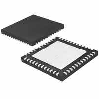
Page 23
... SHADED AREA IS ONLY A REFERENCE FOR PIN 1 LOCATION ON THE TOP AND BOTTOM OF PACKAGE Information furnished by Linear Technology Corporation is believed to be accurate and reliable. However, no responsibility is assumed for its use. Linear Technology Corporation makes no representa- tion that the interconnection of its circuits as described herein will not infringe on existing patent rights. ...
Page 24
... 30pF R FBA 45 6 – I OUT1A U4B LT1469 OUT2A 44 R VOSA 43 R VOSB + OUT2B U4A LT1469 42 2 – I OUT1B – 30pF R GND GND FBB 1007 • PRINTED IN USA © LINEAR TECHNOLOGY CORPORATION 2007 7 V OUTA 1 V OUTB 2753 TA03 2753f ...