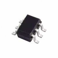
AD5611AKSZ-500RL7 Analog Devices Inc, AD5611AKSZ-500RL7 Datasheet - Page 18

AD5611AKSZ-500RL7
Manufacturer Part Number
AD5611AKSZ-500RL7
Description
IC DAC 10BIT BUFF V-OUT SC70-6
Manufacturer
Analog Devices Inc
Series
nanoDAC™r
Datasheet
1.AD5611AKSZ-500RL7.pdf
(20 pages)
Specifications of AD5611AKSZ-500RL7
Data Interface
SPI™
Package / Case
SC-70-6, SC-88, SOT-363
Mounting Type
Surface Mount
Power Dissipation (max)
500µW
Operating Temperature
-40°C ~ 125°C
Number Of Bits
10
Voltage Supply Source
Single Supply
Settling Time
6µs
Number Of Converters
1
Resolution (bits)
10bit
Sampling Rate
1.7MSPS
Input Channel Type
Serial
Supply Voltage Range - Analog
2.7V To 5.5V
Supply Current
75µA
Digital Ic Case Style
SC-70
Lead Free Status / RoHS Status
Lead free / RoHS Compliant
AD5601/AD5611/AD5621
APPLICATIONS
CHOOSING A REFERENCE AS POWER SUPPLY FOR
THE AD5601/AD5611/AD5621
The AD5601/AD5611/AD5621 come in a tiny SC70 package
with less than a 100 μA supply current. Because of this, the
choice of reference depends on the application requirement. For
space-saving applications, the
package and has excellent drift at 9 ppm/°C (3 ppm/°C in the
R-8 package). It also provides very good noise performance at
3.4 μV p-p in the 0.1 Hz to 10 Hz range.
Because the supply current required by the AD5601/AD5611/
AD5621 is extremely low, the parts are ideal for low supply
applications. The
this case. It requires less than 100 μA of quiescent current and
can, therefore, drive multiple DACs in one system, if required. It
also provides very good noise performance at 8 μV p-p in the
0.1 Hz to 10 Hz range.
Some recommended precision references for use as supplies to
the AD5601/AD5611/AD5621 are listed in Table 7.
Table 7. Precision References for the AD5601/AD5611/AD5621
Part No.
ADR435
ADR425
ADR02
ADR02
ADR395
INTERFACE
Figure 50. ADR395 as Power Supply to the AD5601/AD5611/AD5621
SERIAL
3-WIRE
Initial
Accuracy
(mV max)
±2
±2
±3
±3
±5
7V
SYNC
SCLK
SDIN
ADR395
ADR395
Temp. Drift
(ppm/°C max)
3 (R-8)
3 (R-8)
3 (R-8)
3 (SC70)
9 (TSOT-23)
voltage reference is recommended in
AD5601/AD5611/
ADR02
5V
AD5621
is available in an SC70
0.1 Hz to 10 Hz
Noise (μV p-p typ)
8
3.4
10
10
8
V
OUT
= 0V TO 5V
Rev. C | Page 18 of 20
BIPOLAR OPERATION USING THE
AD5601/AD5611/AD5621
The AD5601/AD5611/AD5621 have been designed for single-
supply operation, but a bipolar output range is also possible
using the circuit shown in Figure 51. The circuit in Figure 51
gives an output voltage range of ±5 V. Rail-to-rail operation at
the amplifier output is achievable using an
the output amplifier.
The output voltage for any input code can be calculated as
where D represents the input code in decimal (0 – 2
With V
This is an output voltage range of ±5 V with 0x0000 corre-
sponding to a −5 V output, and 0x3FFF corresponding to a
+5 V output.
+5V
V
V
Figure 51. Bipolar Operation with the AD5601/AD5611/AD5621
OUT
OUT
DD
= 5 V, R1 = R2 = 10 kΩ
=
=
10µF
⎡
⎢
⎣
⎛
⎜
⎝
V
10
DD
2
×
N
0.1µF
×
D
⎛
⎜
⎝
⎞
⎟
⎠
2
D
−
N
V
AD5601/AD5611/
DD
5
⎞
⎟
⎠
×
V
INTERFACE
R1 = 10kΩ
AD5621
⎛
⎜
⎝
3-WIRE
SERIAL
R1
R1
+
R2
V
OUT
⎞
⎟
⎠
−
AD820
V
R2 = 10kΩ
AD820/
OP295
DD
+5V
–5V
×
⎛
⎜
⎝
or
R2
R1
N
).
OP295
⎞
⎟
⎠
⎤
⎥
⎦
+5V
as


