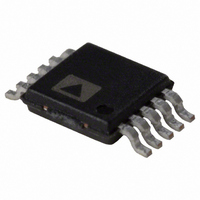
AD5325ARM Analog Devices Inc, AD5325ARM Datasheet - Page 3

AD5325ARM
Manufacturer Part Number
AD5325ARM
Description
IC DAC 12BIT 2WIRE I2C 10-MSOP
Manufacturer
Analog Devices Inc
Datasheet
1.AD5305ARMZ.pdf
(24 pages)
Specifications of AD5325ARM
Rohs Status
RoHS non-compliant
Settling Time
6µs
Number Of Bits
12
Data Interface
I²C, Serial
Number Of Converters
4
Voltage Supply Source
Single Supply
Power Dissipation (max)
5mW
Operating Temperature
-40°C ~ 105°C
Mounting Type
Surface Mount
Package / Case
10-MSOP, Micro10™, 10-uMAX, 10-uSOP
Available stocks
Company
Part Number
Manufacturer
Quantity
Price
Part Number:
AD5325ARMZ
Manufacturer:
ADI/亚德诺
Quantity:
20 000
SPECIFICATIONS
V
Table 1.
Parameter
DC PERFORMANCE
DAC REFERENCE INPUTS
OUTPUT CHARACTERISTICS
DD
AD5305
AD5315
AD5325
Offset Error
Gain Error
Lower Deadband
Offset Error Drift
Gain Error Drift
Power Supply Rejection Ratio
DC Crosstalk
V
V
Reference Feedthrough
Minimum Output Voltage
Maximum Output Voltage
DC Output Impedance
Short-Circuit Current
Power-Up Time
REF
REF
= 2.5 V to 5.5 V, V
Resolution
Relative Accuracy
Differential Nonlinearity
Resolution
Relative Accuracy
Differential Nonlinearity
Resolution
Relative Accuracy
Differential Nonlinearity
Input Range
Input Impedance
2
5
5
3, 4
5
REF
5
= 2 V, R
5
6
6
5
Min
0.25
37
L
= 2 kΩ to GND, C
A Version
Typ
8
±0.15
±0.02
10
±0.5
±0.05
12
±2
±0.2
±0.4
±0.15
20
−12
−5
–60
200
45
>10
−90
0.001
V
0.001
0.5
25
16
2.5
5
DD
−
1
Max
±1
±0.25
±4
±0.5
±16
±1
±3
±1
60
V
DD
L
= 200 pF to GND, all specifications T
Rev. G | Page 3 of 24
Min
0.25
37
B Version
Typ
8
±0.15
±0.02
10
±0.5
±0.05
12
±2
±0.2
±0.4
±0.15
20
−12
−5
–60
200
45
>10
−90
0.001
V
0.001
0.5
25
16
2.5
5
DD
−
1
Max
±0.625
±0.25
±2.5
±0.5
±10
±1
±3
±1
60
V
DD
Unit
Bits
LSB
LSB
Bits
LSB
LSB
Bits
LSB
LSB
% of FSR
% of FSR
mV
ppm of
FSR/°C
ppm of
FSR/°C
dB
μV
V
kΩ
MΩ
dB
V
V
Ω
mA
mA
μs
μs
MIN
to T
AD5305/AD5315/AD5325
MAX
Conditions/Comments
Guaranteed monotonic by design
over all codes
Guaranteed monotonic by design
over all codes
Guaranteed monotonic by design
over all codes
Lower deadband exists only if offset
error is negative
∆V
R
Normal operation
Power-down mode
Frequency = 10 kHz
A measure of the minimum and
maximum drive capability of the
output amplifier
V
V
Coming out of power-down mode
V
Coming out of power-down mode
V
L
DD
DD
DD
DD
= 2 kΩ to GND or V
, unless otherwise noted.
DD
= 5 V
= 3 V
= 5 V
= 3 V
= ±10%
DD


