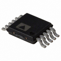
AD5325ARM Analog Devices Inc, AD5325ARM Datasheet - Page 8

AD5325ARM
Manufacturer Part Number
AD5325ARM
Description
IC DAC 12BIT 2WIRE I2C 10-MSOP
Manufacturer
Analog Devices Inc
Datasheet
1.AD5305ARMZ.pdf
(24 pages)
Specifications of AD5325ARM
Rohs Status
RoHS non-compliant
Settling Time
6µs
Number Of Bits
12
Data Interface
I²C, Serial
Number Of Converters
4
Voltage Supply Source
Single Supply
Power Dissipation (max)
5mW
Operating Temperature
-40°C ~ 105°C
Mounting Type
Surface Mount
Package / Case
10-MSOP, Micro10™, 10-uMAX, 10-uSOP
Available stocks
Company
Part Number
Manufacturer
Quantity
Price
Part Number:
AD5325ARMZ
Manufacturer:
ADI/亚德诺
Quantity:
20 000
AD5305/AD5315/AD5325
PIN CONFIGURATION AND FUNCTION DESCRIPTIONS
Table 5. Pin Function Descriptions
Pin No.
1
2
3
4
5
6
7
8
9
10
Mnemonic
V
V
V
V
REFIN
V
GND
SDA
SCL
A0
DD
OUT
OUT
OUT
OUT
A
B
C
D
Description
Power Supply Input. These parts can be operated from 2.5 V to 5.5 V and the supply should be decoupled to GND.
Buffered Analog Output Voltage from DAC A. The output amplifier has rail-to-rail operation.
Buffered Analog Output Voltage from DAC B. The output amplifier has rail-to-rail operation.
Buffered Analog Output Voltage from DAC C. The output amplifier has rail-to-rail operation.
Reference Input Pin for All Four DACs. It has an input range from 0.25 V to V
Buffered Analog Output Voltage from DAC D. The output amplifier has rail-to-rail operation.
Ground Reference Point for All Circuitry on the Part.
Serial Data Line. This is used in conjunction with the SCL line to clock data into or out of the 16-bit input shift
register. It is a bidirectional open-drain data line that should be pulled to the supply with an external pull-up
resistor.
Serial Clock Line. This is used in conjunction with the SDA line to clock data into or out of the 16-bit input shift
register. Clock rates of up to 400 kb/s can be accommodated in the 2-wire interface.
Address Input. Sets the least significant bit of the 7-bit slave address.
V
V
V
REFIN
OUT
OUT
OUT
V
DD
A
B
C
Figure 3. Pin Configuration
1
2
3
4
5
Rev. G | Page 8 of 24
(Not to Scale)
AD5305/
AD5315/
AD5325
TOP VIEW
10
9
8
7
6
A0
SCL
SDA
GND
V
OUT
D
DD
.


