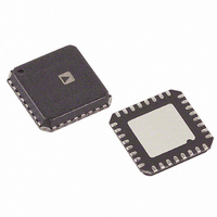
AD9706BCPZ Analog Devices Inc, AD9706BCPZ Datasheet - Page 32

AD9706BCPZ
Manufacturer Part Number
AD9706BCPZ
Description
IC DAC TX 12BIT 175MSPS 32-LFCSP
Manufacturer
Analog Devices Inc
Series
TxDAC®r
Datasheet
1.AD9704BCPZ.pdf
(52 pages)
Specifications of AD9706BCPZ
Settling Time
11ns
Number Of Bits
12
Data Interface
Serial
Number Of Converters
1
Voltage Supply Source
Analog and Digital
Power Dissipation (max)
50mW
Operating Temperature
-40°C ~ 85°C
Mounting Type
Surface Mount
Package / Case
32-LFCSP
Inl ±
1.48LSB
Update Rate
175MSPS
Output Type
Current
Termination Type
SMD
Supply Voltage Max
3.6V
No. Of Bits
12 Bit
Leaded Process Compatible
Yes
Dnl±
1.17LSB
No. Of Dacs
1
Lead Free Status / RoHS Status
Lead free / RoHS Compliant
For Use With
AD9706-EBZ - BOARD EVAL FOR AD9706
Lead Free Status / RoHS Status
Lead free / RoHS Compliant, Lead free / RoHS Compliant
Available stocks
Company
Part Number
Manufacturer
Quantity
Price
Company:
Part Number:
AD9706BCPZ
Manufacturer:
REALTEK
Quantity:
2 300
Part Number:
AD9706BCPZ
Manufacturer:
ADI/亚德诺
Quantity:
20 000
AD9704/AD9705/AD9706/AD9707
SPI REGISTER DESCRIPTIONS
Table 16. SPI CTL—Register 0x00
Mnemonic
SDIODIR
DATADIR
SWRST
LNGINS
PDN
SLEEP
CLKOFF
EXREF
Table 17. DATA—Register 0x02
Mnemonic
DATAFMT
DCLKPOL
DESKEW
CLKDIFF
CALCLK
Table 18. VERSION—Register 0x0D
Mnemonic
VER[3:0]
Table 19. CALMEM—Register 0x0E
Mnemonic
CALMEM[1:0]
DIVSEL[2:0]
Bit No.
7
6
5
4
3
2
1
0
Bit No.
7
4
3
2
0
Bit No.
[3:0]
Bit No.
[5:4]
[2:0]
I
I
I
I
Direction (I/O)
I
I
I
I
Direction (I/O)
I
I
I
I
I
Direction (I/O)
O
Direction (I/O)
O
I
Default
1
0
0
0
0
0
0
0
Default
0000
Default
0
0
0
0
0
000
Default
00
Description
0: SDIO pin configured for input only during data transfer (4-wire interface).
1: SDIO pin configured for input or output during data transfer (3-wire interface).
0: Serial data uses MSB first format.
1: Serial data uses LSB first format.
1: Initiate a software reset; this bit is set to 0 upon reset completion.
0: Use 1 byte preamble (5 address bits).
1: Use 2 byte preamble (13 address bits).
1: Shuts down DAC output current internal band gap reference.
1: DAC output current off.
1: Disables internal master clock.
0: Internal band gap reference.
1: External reference.
Rev. A | Page 32 of 52
Description
Hardware version identifier.
Description
0: Unsigned binary input data format.
1: Twos complement input data format.
0: Data latched on DATACLK rising edge always.
1: Data latched on DATACLK falling edge (only active in DESKEW mode).
0: DESKEW mode disabled.
1: DESKEW mode enabled (adds a register in digital data path to remove
skew in received data; one clock cycle of latency is introduced).
0: Single-ended clock input.
1: Differential clock input.
0: Calibration clock disabled.
1: Calibration clock enabled.
Calibration clock divide ratio from DAC clock rate.
Description
Calibration memory.
00: Uncalibrated.
01: Self-calibration.
10: Not Used.
11: User input.
000: /256.
001: /128.
…
110: /4.
111: /2.


