AD421BNZ Analog Devices Inc, AD421BNZ Datasheet - Page 5
AD421BNZ
Manufacturer Part Number
AD421BNZ
Description
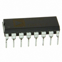
IC DAC SNGL 16BIT 16-DIP
Manufacturer
Analog Devices Inc
Datasheet
1.AD421BRZRL.pdf
(14 pages)
Specifications of AD421BNZ
Data Interface
Serial
Settling Time
8µs
Number Of Bits
16
Number Of Converters
1
Voltage Supply Source
Single Supply
Power Dissipation (max)
1.95mW
Operating Temperature
-40°C ~ 85°C
Mounting Type
Through Hole
Package / Case
16-DIP (0.300", 7.62mm)
Resolution (bits)
16bit
Sampling Rate
125SPS
Input Channel Type
Serial
Supply Current
575µA
Digital Ic Case Style
DIP
No. Of Pins
16
Lead Free Status / RoHS Status
Lead free / RoHS Compliant
Available stocks
Company
Part Number
Manufacturer
Quantity
Price

Part Number:
AD421BNZ
Manufacturer:
ADI/亚德诺
Quantity:
20 000


Pin
No. Mnemonic
1
2
3
4
5
6
7
8
9
10
11
12
13
14
15
16
REV. C
REF OUT1
REF OUT2
REF IN
LV
LATCH
CLOCK
DATA
LOOP RTN
COM
C3
C2
C1
DRIVE
COMP
BOOST
V
CC
Function
Reference Output 1. A precision +1.25 V reference is provided at this pin. It is intended as a precision ref-
erence source for other devices in the transmitter. REF OUT1 is a buffered output capable of providing up
to 0.5 mA to external circuitry. If REF OUT 1 is required to sink current, a resistive load of 100 kΩ to COM
should be added. (See Reference section.)
Reference Output 2. A precision +2.5 V reference is provided at this pin. To operate the AD421 with its
own reference, REF OUT2 should be connected to REF IN. It can also be used as a precision reference
source for other devices in the transmitter. REF OUT2 is a buffered output capable of providing up to
0.5 mA to external circuitry.
Voltage Reference Input. The reference voltage for the AD421 is applied to this pin and it sets the span for
the AD421. The nominal reference voltage for the AD421 is +2.5 V for correct operation. This can be sup-
plied using an external reference source or by using the part’s own REF OUT2 voltage.
Regulated Voltage Control Input. The LV input controls the loop gain of the servo amplifier to set V
With LV connected to COM, the regulator voltage is set to 5 V nominal. If the LV input is connected through
0.01 µF to V
V
DAC Latch Input. Logic Input. A rising edge of the LATCH signal loads the data from the serial input shift
register to the DAC latch and hence updates the output of the DAC. The number of clock cycles provided
between latch pulses determines whether the DAC is in alarm or normal current mode. (See Digital Inter-
face section.)
Data Clock Input. Data on the DATA input is clocked into the shift register on the rising edge of this
CLOCK input. The period of this clock equals the input serial data bit rate. This serial clock rate can be up
to 10 MHz. If 16 clock cycles are provided between LATCH pulses then the data on the DATA input is
accepted as normal 4–20 mA data. If more than 16 clock cycles are provided between LATCH pulses, the
data is assumed to be alarm current data (see Digital Interface section).
Data Input. The data to be loaded to the AD421 input shift register is applied to this input. Data should be
valid on the rising edge of the CLOCK input.
Loop Return Output. LOOP RTN is the return path for current flowing in the current loop.
Common. This is the reference potential for the AD421 analog and digital inputs and outputs and for the
voltage regulator output.
Filtering Capacitor. A low dielectric absorption capacitor ceramic capacitor should be connected between
this pin and COM for internal filtering of the switched current sources.
Filtering Capacitor. See C3 description.
Filtering Capacitor. See C3 description.
Output from the Voltage Regulator Loop. The DRIVE signal controls the external pass transistor to establish and
maintain the correct V
rent is programmed from 4 mA to 20 mA.
Compensation Capacitor Input. A capacitor connected between COMP and DRIVE is required to stabilize
the feedback loop formed with the regulator op amp and the external pass transistor.
This open collector pin sinks the necessary current from the loop so that the current flowing into BOOST
plus the current flowing into COM is equal to the programmed loop current.
Power Supply. V
driven by the external pass transistor. It is used both to bias the AD421 itself and to provide power for the
rest of the smart transmitter circuitry. The LV input determines the regulated voltage output to be either
3 V, 3.3 V or 5 V nominal. Alternatively, a separate power supply can be connected to this pin to power the
AD421. V
CC
, is 3 V nominal.
CC
CC
should be decoupled to COM with a 2.2 µF capacitor.
, the regulated voltage is nominally 3.3 V. With LV connected to V
CC
is the power supply input of the AD421 and it also provides the voltage regulator output,
CC
PIN FUNCTION DESCRIPTIONS
level programmed by the LV inputs while providing the necessary bias as the loop cur-
–5–
CC
the regulated voltage,
AD421
CC
.
Related parts for AD421BNZ
Image
Part Number
Description
Manufacturer
Datasheet
Request
R

Part Number:
Description:
±1.7g Dual-Axis IMEMS Accelerometer Evaluation Board
Manufacturer:
Analog Devices Inc
Datasheet:

Part Number:
Description:
Inertial Sensor Evaluation System
Manufacturer:
Analog Devices Inc
Datasheet:
Part Number:
Description:
Manufacturer:
Analog Devices Inc
Datasheet:
Part Number:
Description:
Manufacturer:
Analog Devices Inc
Datasheet:
Part Number:
Description:
Manufacturer:
Analog Devices Inc
Datasheet:
Part Number:
Description:
Manufacturer:
Analog Devices Inc
Datasheet:
Part Number:
Description:
Manufacturer:
Analog Devices Inc
Datasheet:
Part Number:
Description:
Manufacturer:
Analog Devices Inc
Datasheet:
Part Number:
Description:
Manufacturer:
Analog Devices Inc
Datasheet:
Part Number:
Description:
Manufacturer:
Analog Devices Inc
Datasheet:
Part Number:
Description:
Manufacturer:
Analog Devices Inc
Datasheet:
Part Number:
Description:
Manufacturer:
Analog Devices Inc
Datasheet:
Part Number:
Description:
Manufacturer:
Analog Devices Inc
Datasheet: