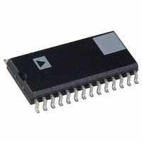
AD9754AR Analog Devices Inc, AD9754AR Datasheet - Page 13

AD9754AR
Manufacturer Part Number
AD9754AR
Description
IC DAC 14BIT 125MSPS HP 28-SOIC
Manufacturer
Analog Devices Inc
Series
TxDAC®r
Datasheet
1.AD9754ARUZ.pdf
(24 pages)
Specifications of AD9754AR
Rohs Status
RoHS non-compliant
Settling Time
35ns
Number Of Bits
14
Data Interface
Parallel
Number Of Converters
1
Voltage Supply Source
Analog and Digital
Power Dissipation (max)
220mW
Operating Temperature
-40°C ~ 85°C
Mounting Type
Surface Mount
Package / Case
28-SOIC (7.5mm Width)
Package
28SOIC W
Resolution
14 Bit
Conversion Rate
125 MSPS
Digital Interface Type
Parallel
Number Of Outputs Per Chip
1
Output Type
Current
Full Scale Error
±5 %FSR
Integral Nonlinearity Error
±3 LSB
Maximum Settling Time
0.035(Typ) us
Available stocks
Company
Part Number
Manufacturer
Quantity
Price
Part Number:
AD9754AR
Manufacturer:
ADI/亚德诺
Quantity:
20 000
Part Number:
AD9754ARU
Manufacturer:
ADI/亚德诺
Quantity:
20 000
Company:
Part Number:
AD9754ARUZ
Manufacturer:
TI
Quantity:
236
Part Number:
AD9754ARUZ
Manufacturer:
ADI/亚德诺
Quantity:
20 000
Part Number:
AD9754ARUZ-REEL7
Manufacturer:
ADI/亚德诺
Quantity:
20 000
INPUT CLOCK AND DATA TIMING RELATIONSHIP
SNR in a DAC is dependent on the relationship between the
position of the clock edges and the point in time at which the
input data changes. The AD9754 is positive edge triggered, and
so exhibits SNR sensitivity when the data transition is close to
this edge. In general, the goal when applying the AD9754 is to
make the data transitions close to the negative clock edge. This
becomes more important as the sample rate increases. Figure 23
shows the relationship of SNR to clock placement.
SLEEP MODE OPERATION
The AD9754 has a power-down function that turns off the
output current and reduces the supply current to less than
8.5 mA over the specified supply range of 2.7 V to 5.5 V and
temperature range. This mode can be activated by applying a
logic level “1” to the SLEEP pin. This digital input also con-
tains an active pull-down circuit that ensures the AD9754 re-
mains enabled if this input is left disconnected. The AD9754
takes less than 50 ns to power down and approximately 5 s to
power back up.
POWER DISSIPATION
The power dissipation, P
several factors, including: (1) AVDD and DVDD, the power
supply voltages; (2) I
f
waveform. The power dissipation is directly proportional to the
analog supply current, I
I
Figure 24, and is insensitive to f
Conversely, I
form, f
show I
(f
DVDD = 3 V, respectively. Note, how I
than a factor of 2 when DVDD is reduced from 5 V to 3 V.
REV. A
CLOCK
DVDD
OUT
Figure 23. SNR vs. Clock Placement @ f
/f
. I
, the update rate; and (4) the reconstructed digital input
CLOCK
DVDD
CLOCK
AVDD
68
64
60
56
52
48
44
40
–8
as a function of full-scale sine wave output ratios
) for various update rates with DVDD = 5 V and
, and digital supply DVDD. Figures 25 and 26
DVDD
is directly proportional to I
–6
TIME (ns) OF DATA CHANGE RELATIVE TO
is dependent on both the digital input wave-
–4
OUTFS
AVDD
D
–2
RISING CLOCK EDGE
, of the AD9754 is dependent on
, the full-scale current output; (3)
, and the digital supply current,
0
CLOCK
2
.
DVDD
F
OUTFS,
4
S
= 125MSPS
is reduced by more
F
S
6
OUT
= 65MSPS
as shown in
= 10 MHz
8
10
–13–
18
16
14
12
10
35
30
25
20
15
10
8
6
4
2
0
0.01
8
6
4
2
0
5
0.01
Figure 25. I
Figure 26. I
2
4
Figure 24. I
6
DVDD
DVDD
RATIO (f
8
RATIO (f
vs. Ratio @ DVDD = 5 V
vs. Ratio @ DVDD = 3 V
I
OUTFS
10
AVDD
CLOCK
0.1
CLOCK
0.1
– mA
12
vs. I
/f
/f
OUT
OUT
14
)
)
OUTFS
16
125MSPS
100MSPS
50MSPS
25MSPS
5MSPS
125MSPS
100MSPS
50MSPS
25MSPS
5MSPS
AD9754
18
1
20
1


