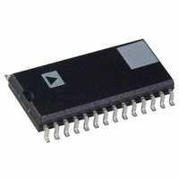
AD9754AR Analog Devices Inc, AD9754AR Datasheet - Page 5

AD9754AR
Manufacturer Part Number
AD9754AR
Description
IC DAC 14BIT 125MSPS HP 28-SOIC
Manufacturer
Analog Devices Inc
Series
TxDAC®r
Datasheet
1.AD9754ARUZ.pdf
(24 pages)
Specifications of AD9754AR
Rohs Status
RoHS non-compliant
Settling Time
35ns
Number Of Bits
14
Data Interface
Parallel
Number Of Converters
1
Voltage Supply Source
Analog and Digital
Power Dissipation (max)
220mW
Operating Temperature
-40°C ~ 85°C
Mounting Type
Surface Mount
Package / Case
28-SOIC (7.5mm Width)
Package
28SOIC W
Resolution
14 Bit
Conversion Rate
125 MSPS
Digital Interface Type
Parallel
Number Of Outputs Per Chip
1
Output Type
Current
Full Scale Error
±5 %FSR
Integral Nonlinearity Error
±3 LSB
Maximum Settling Time
0.035(Typ) us
Available stocks
Company
Part Number
Manufacturer
Quantity
Price
Part Number:
AD9754AR
Manufacturer:
ADI/亚德诺
Quantity:
20 000
Part Number:
AD9754ARU
Manufacturer:
ADI/亚德诺
Quantity:
20 000
Company:
Part Number:
AD9754ARUZ
Manufacturer:
TI
Quantity:
236
Part Number:
AD9754ARUZ
Manufacturer:
ADI/亚德诺
Quantity:
20 000
Part Number:
AD9754ARUZ-REEL7
Manufacturer:
ADI/亚德诺
Quantity:
20 000
Pin No.
1
2–13
14
15
16
17
18
19, 25
20
21
22
23
24
26
27
28
REV. A
Name
DB13
DB12–DB1 Data Bits 1–12.
DB0
SLEEP
REFLO
REFIO
FS ADJ
NC
ACOM
IOUTB
IOUTA
ICOMP
AVDD
DCOM
DVDD
CLOCK
Description
Most Significant Data Bit (MSB).
Least Significant Data Bit (LSB).
Power-Down Control Input. Active High. Contains active pull-down circuit; it may be left unterminated if
not used.
Reference Ground when Internal 1.2 V Reference Used. Connect to AVDD to disable internal reference.
Reference Input/Output. Serves as reference input when internal reference disabled (i.e., Tie REFLO to
AVDD). Serves as 1.2 V reference output when internal reference activated (i.e., Tie REFLO to ACOM).
Requires 0.1 F capacitor to ACOM when internal reference activated.
Full-Scale Current Output Adjust.
No Connect.
Analog Common.
Complementary DAC Current Output. Full-scale current when all data bits are 0s.
DAC Current Output. Full-scale current when all data bits are 1s.
Internal Bias Node for Switch Driver Circuitry. Decouple to ACOM with 0.1 F capacitor.
Analog Supply Voltage (+4.5 V to +5.5 V).
Digital Common.
Digital Supply Voltage (+2.7 V to +5.5 V).
Clock Input. Data latched on positive edge of clock.
PIN FUNCTION DESCRIPTIONS
(MSB) DB13
(LSB) DB0
PIN CONFIGURATION
DB12
DB11
DB10
DB9
DB8
DB7
DB6
DB5
DB4
DB3
DB2
DB1
10
11
12
13
14
NC = NO CONNECT
1
2
3
4
5
6
7
8
9
(Not to Scale)
TOP VIEW
AD9754
–5–
28
27
26
25
24
23
22
21
20
19
18
17
16
15
CLOCK
DVDD
DCOM
NC
AVDD
IOUTA
IOUTB
ACOM
NC
FS ADJ
REFIO
REFLO
SLEEP
ICOMP
AD9754


