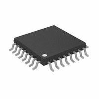
AD5763CSUZ-REEL7 Analog Devices Inc, AD5763CSUZ-REEL7 Datasheet - Page 19

AD5763CSUZ-REEL7
Manufacturer Part Number
AD5763CSUZ-REEL7
Description
DAC 16BIT DUAL 5V 2LSB 32-TQFP
Manufacturer
Analog Devices Inc
Datasheet
1.AD5763CSUZ.pdf
(28 pages)
Specifications of AD5763CSUZ-REEL7
Design Resources
High Accuracy, Bipolar Voltage Output Digital-to-Analog Conversion Using AD5763 (CN0074)
Settling Time
8µs
Number Of Bits
16
Data Interface
Serial
Number Of Converters
2
Voltage Supply Source
Dual ±
Power Dissipation (max)
45mW
Operating Temperature
-40°C ~ 105°C
Mounting Type
Surface Mount
Package / Case
32-TQFP, 32-VQFP
Lead Free Status / RoHS Status
Lead free / RoHS Compliant
Available stocks
Company
Part Number
Manufacturer
Quantity
Price
Company:
Part Number:
AD5763CSUZ-REEL7
Manufacturer:
Analog Devices Inc
Quantity:
10 000
FUNCTION REGISTER
The function register is addressed by setting the three REG bits to 000. The values written to the address bits and the data bits determine
the function addressed. The functions available via the function register are outlined in Table 10 and Table 11.
Table 10. Function Register Options
REG2
0
0
0
0
Table 11. Explanation of Function Register Options
Option
NOP
Local-Ground-
D0/D1 Direction
D0/D1 Value
SDO Disable
Clear
Load
DATA REGISTER
The data register is addressed by setting the three REG bits to 010. The DAC address bits select with which DAC channel the data transfer
is to take place (see Table 9). The data bits are in Position DB15 to Position DB0 as shown in Table 12.
Table 12. Programming the Data Register
REG2
0
COARSE GAIN REGISTER
The coarse gain register is addressed by setting the three REG bits to 011. The DAC address bits select with which DAC channel the data
transfer is to take place (see Table 9). The coarse gain register is a 2-bit register and allows the user to select the output range of each DAC
as shown in Table 13 and Table 14.
Table 13. Programming the Coarse Gain Register
REG2
0
Table 14. Output Range Selection
Output Range
±4.096 V (Default)
±4.20103 V
±4.31158 V
Offset Adjust
REG1
0
0
0
0
REG1
1
REG0
0
0
0
0
REG1
1
Description
No operation instruction used in readback operations.
Set by the user to enable local-ground-offset adjust function. Cleared by the user to disable local-ground-offset adjust
function (default). See the Design Features section for further details.
Set by the user to enable D0, D1 as outputs. Cleared by the user to enable D0, D1 as inputs (default). See the Design
Features section for further details.
I/O port status bits. Logic values written to these locations determine the logic outputs on the D0 and D1 pins when
configured as outputs. These bits indicate the status of the D0 and D1 pins when the I/O port is active as an input.
When enabled as inputs, these bits are don’t cares during a write operation.
Set by the user to disable the SDO output. Cleared by the user to enable the SDO output (default).
Addressing this function resets the DAC outputs to 0 V in twos complement mode and negative full scale in binary mode.
Addressing this function updates the DAC registers and, consequently, the analog outputs.
A2
0
0
1
1
A1
0
0
0
0
REG0
1
A0
0
1
0
1
REG0
0
DB15:DB6
Don’t care
A2
DAC address
A2
DB5
Local-ground-offset
adjust
A1
Rev. A | Page 19 of 28
DAC address
A0
A1
Clear, data = don’t care
DB4
D1
direction
Load, data = don’t care
NOP, data = don’t care
CG1
0
0
1
A0
DB15:DB2
Don’t care
DB3
D1
value
DB2
D0
direction
16-bit DAC data
DB15 … DB0
CG0
0
1
0
DB1
CG1
DB1
D0
value
AD5763
DB0
CG0
DB0
SDO
disable


