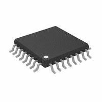
AD5763CSUZ-REEL7 Analog Devices Inc, AD5763CSUZ-REEL7 Datasheet - Page 23

AD5763CSUZ-REEL7
Manufacturer Part Number
AD5763CSUZ-REEL7
Description
DAC 16BIT DUAL 5V 2LSB 32-TQFP
Manufacturer
Analog Devices Inc
Datasheet
1.AD5763CSUZ.pdf
(28 pages)
Specifications of AD5763CSUZ-REEL7
Design Resources
High Accuracy, Bipolar Voltage Output Digital-to-Analog Conversion Using AD5763 (CN0074)
Settling Time
8µs
Number Of Bits
16
Data Interface
Serial
Number Of Converters
2
Voltage Supply Source
Dual ±
Power Dissipation (max)
45mW
Operating Temperature
-40°C ~ 105°C
Mounting Type
Surface Mount
Package / Case
32-TQFP, 32-VQFP
Lead Free Status / RoHS Status
Lead free / RoHS Compliant
Available stocks
Company
Part Number
Manufacturer
Quantity
Price
Company:
Part Number:
AD5763CSUZ-REEL7
Manufacturer:
Analog Devices Inc
Quantity:
10 000
LOCAL GROUND OFFSET ADJUST
The AD5763 incorporates a local-ground-offset adjust feature
which, when enabled in the function register, adjusts the DAC
outputs for voltage differences between the individual DAC
ground pins and the REFGND pin ensuring that the DAC
output voltages are always with respect to the local DAC
ground pin. For instance, if Pin AGNDA is at 5 mV with
respect to the REFGND pin and VOUTA is measured with
respect to AGNDA, then a −5 mV error results, enabling the
local-ground-offset adjust feature which adjusts VOUTA by
+5 mV, eliminating the error.
POWER-ON STATUS
The AD5763 has multiple power supply and digital input pins.
It is important to consider the sequence in which the pins are
powered up to ensure the AD5763 powers-on in the required
state. The outputs will power-on either clamped to AGNDx,
driving 0 V, or driving negative full-scale output (−4.096 V)
depending on how the BIN/ 2sCOMP , CLR , and LDAC pins
are configured during power-up. If the CLR pin is connected to
DGND, it causes the DAC registers to be loaded with 0x0000
and the outputs to be updated. Consequently, the outputs are
Rev. A | Page 23 of 28
loaded with 0 V if BIN/ 2sCOMP is connected to DGND or
negative full-scale (−4.096 V) if BIN/ 2sCOMP is connected to
DV
binary voltages for the digital code 0x0000. During power-up
the state of the LDAC pin has an identical effect to that of the
CLR pin. If both the CLR and LDAC pins are connected to
DV
AGNDx and remain so until a valid write is made to the device.
Table 19 outlines the possible output power-on states.
Table 19. Output Power-On State
BIN/ 2sCOMP
DGND
DGND
DGND
DGND
DV
DV
DV
DV
CC
CC
CC
CC
CC
CC
corresponding respectively to the twos complement and
during power-up the outputs power-on clamped to
CLR
DGND
DGND
DV
DV
DGND
DGND
DV
DV
CC
CC
CC
CC
LDAC
DGND
DV
DGND
DV
DGND
DV
DGND
DV
CC
CC
CC
CC
V
0 V
0 V
0 V
Clamped to AGNDx
−4.096 V
−4.096 V
−4.096 V
Clamped to AGNDx
OUT
at Power-On
AD5763


