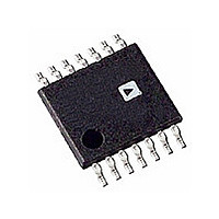
ADM1073ARU-REEL7 Analog Devices Inc, ADM1073ARU-REEL7 Datasheet - Page 15

ADM1073ARU-REEL7
Manufacturer Part Number
ADM1073ARU-REEL7
Description
Manufacturer
Analog Devices Inc
Datasheet
1.ADM1073ARU-REEL7.pdf
(24 pages)
Specifications of ADM1073ARU-REEL7
Linear Misc Type
Negative Voltage
Family Name
ADM1073
Package Type
TSSOP
Operating Supply Voltage (min)
-18V
Operating Supply Voltage (max)
-80V
Operating Temperature (min)
-40C
Operating Temperature (max)
85C
Operating Temperature Classification
Industrial
Product Depth (mm)
4.4mm
Product Height (mm)
1mm
Product Length (mm)
5mm
Mounting
Surface Mount
Pin Count
14
Lead Free Status / Rohs Status
Not Compliant
SENSE
The SENSE pin is used for sensing the voltage across an
external power sense resistor. This voltage is differentially
measured with respect to V
If SENSE is lower than 100 mV (after the soft start time), the
GATE pin is allowed to increase up to 12 V to provide
maximum FET enhancement. If the current increases such that
the SENSE pin tries to go above 100 mV, the GATE pin is
controlled in a feedback loop to ensure that the voltage across
the sense resistor is regulated at exactly 100 mV.
SENSE RESISTOR
The ADM1073’s current limiting function can operate at
different current levels. The current limit is determined by
selection of the sense resistor, R
maximum allowable load current (I
and maximum inrush currents (I
related to the value of R
Table 4. Minumum and Maximum Inrush Current and Load
Current Levels for Different Values of R
R
5
10
15
18
22
33
47
51
68
75
90
SOFT START (SS PIN)
The SS pin is used to determine the inrush current profile.
A capacitor should be attached to this pin. Whenever the FET
is requested to turn on, the SS pin is held at ground until the
SENSE pin reaches a few mV. A current source is then turned
on, which linearly ramps the capacitor up to 2.5 V. The reference
voltage for the GATE linear control amplifier is derived from
the soft start voltage, such that the inrush linear current limit is
defined as
Overdriving the SS Pin
The SS pin can be overdriven externally from 0.360 V to 1.95 V
to offset the current limit control loop threshold from 18 mV to
100 mV. This allows different current limits to be selected at
different points of operation without using multiple sense
resistors. The current limit voltage is clamped at 100 mV
maximum.
SENSE
I
(mΩ)
LIMIT
=
V
SOFT
_
I
17.20
8.60
5.73
4.78
3.91
2.61
1.83
1.69
1.26
1.15
0.96
LOAD(MAX)
START
SENSE
/
EE
.
20
, and used to control the GATE.
(A)
×
SENSE
R
LIMIT(MIN)
SENSE
LOAD(MAX)
. Table 4 shows how the
I
19.40
9.70
6.47
5.39
4.41
2.94
2.06
1.90
1.43
1.29
1.08
LIMIT(MIN)
and I
SENSE
) and the minimum
(A)
LIMIT(MAX)
I
20.60
10.30
6.87
5.72
4.68
3.12
2.19
2.02
1.51
1.37
1.14
LIMIT(MAX)
) are
(A)
Rev. 0 | Page 15 of 24
GATE
Analog output for driving the external FET gate. This pin is
switched to V
the FET is at the programmed inrush current limit, and is
switched to V
current capability is small to provide slow controlled turn-on,
and the sink current capability is large to provide fast turn-off.
V
Positive supply pin. This current-driven supply is shunt-
regulated at 12.3 V internally, and should be connected to the
most positive input supply terminal (usually −48 V RTN or 0 V)
through a dropper resistor. The resistor should be chosen such
that it always supplies enough current to overcome the
maximum quiescent supply current of the chip. Default R
30 kΩ.
V
Negative supply input. This pin should be connected directly to
the most negative input supply terminal (−48 V). This pin is
also used for differentially sensing across the external power
resistor, and should, therefore, be connected as close to the sense
resistor as possible. (See the Kelvin Sense Resistor Connection
section.)
TIMING CONTROL—TIMER
The TIMER pin is an analog pin that determines the maximum
on-time when the FET is in linear current limit, and controls
the PWM duty cycle for pulsed load capacitor charging. A
capacitor should be attached to this pin. When the FET is in
current limit, a 19 µA current source charges the external
capacitor. If the FET is still in current limit when the TIMER
capacitor reaches 2.5 V, the GATE driver is turned off and a
1 µA discharge current sink is turned on. The GATE remains
low until the TIMER capacitor is reduced to 0.5 V. At this point,
the GATE pin is turned on again. If the FET goes back into
current limit, the TIMER recharging starts again.
The PWM duty cycle is set at 6% default level by the size of
these two current sources. Adding a resistor from TIMER to V
decreases the duty cycle. Adding a resistor from TIMER to V
increases the duty cycle.
In addition, a current proportional to the current into the
DRAIN pin is added to the charging current. The additional
current varies linearly with DRAIN voltage. This reduces the
maximum on-time and the percentage PWM duty cycle when
there is a large voltage across the FET.
IN
EE
EE
IN
when the FET is fully enhanced. The source
when the FET is off, is linearly controlled when
ADM1073
DROP
IN
=
EE


