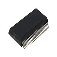
ICS87158AF IDT, Integrated Device Technology Inc, ICS87158AF Datasheet

ICS87158AF
Specifications of ICS87158AF
Related parts for ICS87158AF
ICS87158AF Summary of contents
Page 1
G D ENERAL ESCRIPTION The ICS87158 is a high performance 1-to-6 LVPECL-to- HCSL/LVCMOS ClockGenerator. The ICS87158 has one differential input (which can accept LVDS, LVPECL, LVHSTL, SSTL, HCSL), six differential HCSL output pairs and two complementary LVCMOS/LVTTLoutputs. The six HCSL ...
Page 2
ABLE IN ESCRIPTIONS ...
Page 3
ABLE IN HARACTERISTICS ...
Page 4
BSOLUTE AXIMUM ATINGS Supply Voltage Inputs Outputs Package Thermal Impedance Lead TSSOP 48 Lead SSOP Storage Temperature, T STG T 4A ABLE OWER UPPLY HARACTERISTICS ...
Page 5
T 4D. HCSL DC C ABLE HARACTERISTICS ...
Page 6
P ARAMETER 3.3V± HCSL GND 0V 3.3V HCSL UTPUT OAD EST V DD nPCLK V Cross Points PP PCLK GND IFFERENTIAL NPUT EVEL 80% Clock 20% Outputs ...
Page 7
HOST_Nx HOST_Px PERIOD t PW odc = t PERIOD HCSL UTPUT UTY YCLE ULSE nPCLK PCLK HOST_Nx HOST_Px ROPAGATION ELAY 87158AG 1- -6, LVPECL- TO MREF, nMREF x ...
Page 8
IRING THE IFFERENTIAL NPUT TO Figure 1 shows how the differential input can be wired to accept single ended levels. The reference voltage V_REF = V generated by the bias resistors R1, R2 and C1. This bias ...
Page 9
LVPECL LOCK NPUT NTERFACE The PCLK /nPCLK accepts LVPECL, CML, SSTL and other differential signals. Both V and V SWING input requirements. Figures show interface and V CMR examples for the PCLK/nPCLK input driven ...
Page 10
S E CHEMATIC XAMPLE Figure 3 shows an example of the ICS87158 LVPECL to HCSL Clock Generator schematic. In this example, the ICS87158 is configured as follows: PWR_DWN Mult_[1:0] = 10, Rref = 475 , IREF = 2.32mA, ...
Page 11
Power and Ground This section provides a layout guide related to power, ground and placement of bypass capacitors for a high- speed digital IC. This layout guide is a general recommen- dation. The actual board design will depend on the ...
Page 12
OGIC ONTROL NPUT The logic input control signals are 3.3V LVCMOS compatible. The logic control input contains ESD diodes and either pull-up or pull-down resistor as shown in Figure 5. The data sheet pro- vides pull-up or ...
Page 13
T 6A ABLE VS IR LOW ABLE OR JA Single-Layer PCB, JEDEC Standard Test Boards Multi-Layer PCB, JEDEC Standard Test Boards NOTE: Most modern PCB designs use multi-layered boards. The data in the second row ...
Page 14
ACKAGE UTLINE UFFIX FOR T 6A ABLE ACKAGE IMENSIONS ...
Page 15
ABLE RDERING NFORMATION ...
Page 16
...
Page 17
We’ve Got Your Timing Solution. 6024 Silver Creek Valley Road San Jose, CA 95138 © 2010 Integrated Device Technology, Inc. All rights reserved. Product specifications subject to change without notice. IDT, the IDT logo, ICS and HiPerClockS are trademarks of ...


