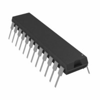
DAC8248FP Analog Devices Inc, DAC8248FP Datasheet - Page 11

DAC8248FP
Manufacturer Part Number
DAC8248FP
Description
IC DAC 12BIT DUAL BUFFERD 24-DIP
Manufacturer
Analog Devices Inc
Datasheet
1.DAC8248FPZ.pdf
(16 pages)
Specifications of DAC8248FP
Rohs Status
RoHS non-compliant
Settling Time
1µs
Number Of Bits
12
Data Interface
Parallel
Number Of Converters
2
Voltage Supply Source
Single Supply
Power Dissipation (max)
50µW
Operating Temperature
-40°C ~ 85°C
Mounting Type
Through Hole
Package / Case
24-DIP (0.300", 7.62mm)
Available stocks
Company
Part Number
Manufacturer
Quantity
Price
Part Number:
DAC8248FP
Manufacturer:
ADI/亚德诺
Quantity:
20 000
L
L
L
L
H
H
H
H
X
X
X
X
L = Low, H = High, X = Don’t Care, WR = Registers Being Loaded, LAT = Registers Latched.
AUTOMATIC DATA TRANSFER MODE
Data may be transferred automatically from the input register to
the DAC register. The first cycle loads the first data byte into
the input register; the second cycle loads the second data byte
and simultaneously transfers the full 12-bit data word to the
DAC register. It takes four cycles to load and transfer two com-
plete digital words for both DAC’s, see Figure 4 (Four Cycle
Update Timing Diagram) and the Mode Selection Table.
STROBED DATA TRANSFER MODE
Strobed data transfer allows the full 12-bit digital word to be
loaded into the input registers and transferred to the DAC regis-
ters at a later time. This transfer mode requires five cycles: four
to load two new data words into both DACs, and the fifth to
transfer all data into the DAC registers. See Figure 5 (Five Cycle
Update Timing Diagram) and the Mode Selection Table.
REV. B
DAC A/B
DIGITAL INPUTS
WR
L
L
L
L
L
L
L
L
H
H
X
H
LSB/MSB
L
L
H
H
L
L
H
H
X
X
X
X
RESET
H
H
H
H
H
H
H
H
H
H
L
g
LDAC LSB
H
L
H
L
H
L
H
L
H
L
X
X
Figure 6. Input Control Logic
MODE SELECTION TABLE
Input Register
WR
WR
LAT
LAT
LAT
LAT
LAT
LAT
LAT
LAT
ALL REGISTERS ARE RESET TO ZEROS
ZEROS ARE LATCHED IN ALL REGISTERS
–11–
Strobed data transfer separating data loading and transfer op-
erations serves two functions: the DAC output updating may be
more precisely controlled, and multiple DACs in a multiple
DAC system can be updated simultaneously.
RESET
The DAC8248 comes with a RESET pin that is useful in system
calibration cycles and/or during system power-up. All registers
are reset to zero when RESET is low, and latched at zero on the
rising edge of the RESET signal when WRITE is high.
INTERFACE CONTROL LOGIC
The DAC8248’s control logic is shown in Figure 6. This cir-
cuitry interfaces with the system bus and controls the DAC
functions.
REGISTER STATUS
DAC A
MSB
LAT
LAT
WR
WR
LAT
LAT
LAT
LAT
LAT
LAT
DAC
Register
LAT
WR
WR
LAT
WR
LAT
WR
LAT
WR
LAT
Input Register
LSB
LAT
LAT
LAT
LAT
WR
WR
LAT
LAT
LAT
LAT
DAC B
MSB
LAT
LAT
LAT
LAT
LAT
LAT
WR
WR
LAT
LAT
DAC8248
DAC
Register
LAT
WR
WR
WR
LAT
WR
LAT
WR
LAT
LAT


