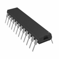
DAC8248FP Analog Devices Inc, DAC8248FP Datasheet - Page 9

DAC8248FP
Manufacturer Part Number
DAC8248FP
Description
IC DAC 12BIT DUAL BUFFERD 24-DIP
Manufacturer
Analog Devices Inc
Datasheet
1.DAC8248FPZ.pdf
(16 pages)
Specifications of DAC8248FP
Rohs Status
RoHS non-compliant
Settling Time
1µs
Number Of Bits
12
Data Interface
Parallel
Number Of Converters
2
Voltage Supply Source
Single Supply
Power Dissipation (max)
50µW
Operating Temperature
-40°C ~ 85°C
Mounting Type
Through Hole
Package / Case
24-DIP (0.300", 7.62mm)
Available stocks
Company
Part Number
Manufacturer
Quantity
Price
Part Number:
DAC8248FP
Manufacturer:
ADI/亚德诺
Quantity:
20 000
The binary-weighted currents are switched between I
AGND by the transistor switches. Selection between I
AGND is determined by the digital input code. It is important
to keep the voltage difference between I
nals as close to zero as practical to preserve data sheet limits. It
is easily accomplished by connecting the DAC’s AGND to the
noninverting input of an operational amplifier and I
inverting input. The amplifier’s feedback resistor can be elimi-
nated by connecting the op amp’s output directly to the DAC’s
R
R
sion for the DAC’s output current.
The output voltage is dependent on the DAC’s digital input
code and V
where D is the digital input code integer number that is between
0 and 4095.
The DAC’s input resistance, R
value, R. This means that V
voltage or current, ac or dc (positive or negative). It is recom-
mended that a low temperature-coefficient external R
be used if a current source is employed.
The DAC’s output capacitance (C
varies from 90 pF (all digital inputs low) to 120 pF (all digital
inputs high).
To ensure accuracy over the full operating temperature range,
permanently turned “ON” MOS transistor switches were in-
cluded in series with the feedback resistor (R
ladder’s terminating resistor (see Figure 1). The gates of these
NMOS transistors are internally connected to V
turned “OFF” (open) if V
ing the DAC’s R
must be applied before or at the same time as the op amp’s sup-
ply; this will prevent the op amp’s output from becoming “open
circuited” and swinging to either rail. In addition, some applica-
tions require the DAC’s ladder resistance to fall within a certain
range and are measured at incoming inspection; V
applied before these measurements can be made.
REV. B
FB
FB
). The amplifier also provides the current-to-voltage conver-
terminal (by using the DAC’s internal feedback resistor,
Figure 2. N-Channel Current Steering Switch
REF
, and is given by:
FB
resistor to close its feedback loop, then V
V
OUT
DD
= V
REF
is not applied. If an op amp is us-
REF
REF
can be driven by a reference
, is always equal to a constant
OUT
D/4096
) is code dependent and
OUT
and AGND termi-
FB
) and the R-2R
DD
DD
and will be
OUT
OUT
must be
FB
OUT
to the
resistor
and
and
DD
–9–
DIGITAL SECTION
The DAC8248’s digital inputs are TTL compatible at V
and CMOS compatible at V
convert TTL and CMOS input logic levels into voltage levels that
will drive the internal circuitry. The DAC8248 can use +5 V
CMOS logic levels with V
will increase to approximately 5 mA–6 mA.
Figure 3 shows the DAC’s digital input structure for one bit.
This circuitry drives the DAC registers. Digital controls, and
circuitry.
The digital inputs are electrostatic-discharge (ESD) protected
with two internal distributed diodes as shown in Figure 3; they
are connected between V
cal input current of less than 1 nA.
The digital inputs are CMOS inverters and draw supply current
when operating in their linear region. Using a +5 V supply, the
linear region is between +1.2 V to +2.8 V with current peaking
at +1.8 V. Using a +15 V supply, the linear region is from
+1.2 V to +12 V (current peaking at +3.9 V). It is recom-
mended that the digital inputs be operated as close to the power
supply voltage and DGND as is practically possible; this will
keep supply currents to a minimum. The DAC8248 may be
operated with any supply voltage between the range of +5 V to
+15 V and still perform to data sheet limits.
The DAC8248’s 8-bit wide data port loads a 12-bit word in two
bytes: 8-bits then 4-bits (or 4-bits first then 8-bits, at users dis-
cretion) in a right justified data format. This data is loaded into
the input registers with the LSB/MSB and WR control pins.
Data transfer from the input registers to the DAC registers can
be automatic. It can occur upon loading of the second data byte
into the input register, or can occur at a later time through a
strobed transfer using the LDAC control pin.
, shown are generated from the DAC’s input control logic
Figure 3. Digital Input Structure For One Bit
DD
DD
DD
and DGND. Each input has a typi-
= +12 V; however, supply current
= +15 V. They were designed to
DAC8248
DD
= +5 V


