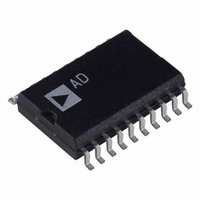
DAC8426FS Analog Devices Inc, DAC8426FS Datasheet - Page 2

DAC8426FS
Manufacturer Part Number
DAC8426FS
Description
IC DAC 8BIT QUAD W/V-REF 20-SOIC
Manufacturer
Analog Devices Inc
Datasheet
1.DAC8426FSZ.pdf
(12 pages)
Specifications of DAC8426FS
Settling Time
3µs
Rohs Status
RoHS non-compliant
Number Of Bits
8
Number Of Converters
4
Voltage Supply Source
Dual ±
Power Dissipation (max)
210mW
Operating Temperature
-40°C ~ 85°C
Mounting Type
Surface Mount
Package / Case
20-SOIC (7.5mm Width)
Resolution (bits)
8bit
Data Interface
CMOS, Parallel
Digital Ic Case Style
SOIC
No. Of Pins
20
Operating Temperature Range
-55°C To +125°C
Update Rate
0.333MSPS
Lead Free Status / RoHS Status
Contains lead / RoHS non-compliant
Available stocks
Company
Part Number
Manufacturer
Quantity
Price
Part Number:
DAC8426FSZ
Manufacturer:
ADI/亚德诺
Quantity:
20 000
ELECTRICAL CHARACTERISTICS
applies for DAC8426AR/BR, T
DAC8426AR/BR, T
Parameter
DAC OUTPUT
DYNAMIC PERFORMANCE
SWITCHING CHARACTERISTICS
NOTES
1
2
3
4
5
6
Specifications subject to change without notice.
DAC8426–SPECIFICATIONS
Parameter
STATIC PERFORMANCE
REFERENCE OUTPUT
DIGITAL INPUTS
POWER SUPPLIES
Includes Full-Scale Error, Relative Accuracy, and Zero Code Error. Note 1 LSB = 0.39% error.
All devices guaranteed monotonic over the full operating temperature range.
Guaranteed and not subject to production test.
Digital inputs V
P
Typicals represent measured characteristics at T
DISS
Output Current (Source)
Output Current (Sink)
Minimum Load Resistance
V
V
Digital Crosstalk
Address To Write Setup Time
Address To Write Hold Time
Data Valid To Write Setup Time
Data Valid To Write Hold Time
Write Pulse Width
Resolution
Total Unadjusted Error
Relative Accuracy
Differential Nonlinearity
Full-Scale Temperature Coefficient
Zero Scale Error
Zero Scale Error
Output Voltage
Temperature Coefficient
Load Regulation
Line Regulation
Output Noise
Output Current
Logic Input “0”
Logic Input “1”
Input Current
Input Capacitance
Positive Supply Current
Negative Supply Current
Power Dissipation
Power Supply Sensitivity
OUT
OUT
(Positive or Negative)
Temperature Coefficient
calculated by I
Slew Rate
Settling Time
IN
= V
3
A
DD
= –40 C to +85 C applies for DAC8426ER/EP/FR/FP/FS, unless otherwise noted.
INL
5
3
V
or V
DD
3
.
INH
1
4
2
3
4
A
; V
= –40 C to +85 C applies for DAC8426ER/EP/FR/FP/FS, unless otherwise noted.)
OUT
3
and V
3
REF
A
OUT unloaded.
= +25 C.
I
I
R
SR
t
Q
t
t
t
t
t
AS
AH
DS
DH
WR
Symbol
OUT
OUT
S
Symbol
N
TUE
INL
DNL
TCG
V
TCV
V
TCV
LD
LN
e
I
V
V
I
C
I
I
P
P
L(MIN)
REF
IN
DD
SS
n
DISS
SS
ZSE
REF
INL
INH
IN
rms
REG
REG
SOURCE
SINK
OUT
OUT
ZS
REF
FS
V
DD
OUT
= +15 V
(V
DD
= +15 V
Conditions
Digital In = All Ones
Digital In = All Zeroes V
Digital In = All Ones
To 1/2 LSB, R
Conditions
Includes Reference
Includes Reference
Dual Supply
No Load
f = 0.1 Hz to 10 Hz
V
Dual Supply
I
V
V
V
IN
L
–2–
10%, AGND = DGND = 0 V, V
DD
REF
DD
= 5 mA
= 0 V or V
OUT < 40 mV
= 5%
10%
10%, AGND = DGND = 0 V, V
DD
L
= 2 k
SS
A, E
B, F
A, E
B, F
V
A, E
B, F
V
SS
SS
= –5 V
= –5 V
= –5 V
SS
= 0 V, T
SS
= 0 V, T
A
10
350
2
0
0
70
10
50
Min
8
9.96
9.92
5
2.4
Min
= –55 C to +125 C applies for
A
= –55 C to +125 C
Typ
25
10
20
0.02
0.008
3
7
0.1
4
6
4
90
0.0002
Typ
450
4
3
10
6
0.04
10
8
14
Max
20
10.04
10.08
0.1
10
0.8
10
210
0.01
Max
1
2
1/2
1
1
REV. C
Units
Bits
LSB
LSB
LSB
LSB
LSB
ppm/ C
mV
V
V
ppm/ C
%/mA
%/V
mA
V
V
pF
mA
mA
mW
%/%
Units
mA
k
V/ s
nVs
ns
ns
ns
ns
ns
V/ C
V p-p
A
A
s


