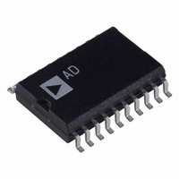
DAC8426FS Analog Devices Inc, DAC8426FS Datasheet - Page 8

DAC8426FS
Manufacturer Part Number
DAC8426FS
Description
IC DAC 8BIT QUAD W/V-REF 20-SOIC
Manufacturer
Analog Devices Inc
Datasheet
1.DAC8426FSZ.pdf
(12 pages)
Specifications of DAC8426FS
Settling Time
3µs
Rohs Status
RoHS non-compliant
Number Of Bits
8
Number Of Converters
4
Voltage Supply Source
Dual ±
Power Dissipation (max)
210mW
Operating Temperature
-40°C ~ 85°C
Mounting Type
Surface Mount
Package / Case
20-SOIC (7.5mm Width)
Resolution (bits)
8bit
Data Interface
CMOS, Parallel
Digital Ic Case Style
SOIC
No. Of Pins
20
Operating Temperature Range
-55°C To +125°C
Update Rate
0.333MSPS
Lead Free Status / RoHS Status
Contains lead / RoHS non-compliant
Available stocks
Company
Part Number
Manufacturer
Quantity
Price
Part Number:
DAC8426FSZ
Manufacturer:
ADI/亚德诺
Quantity:
20 000
DAC8426
The outputs can withstand an indefinite short-circuit to AGND
to typically 50 mA. The output may also be shorted to any volt-
age between V
exceed the device maximum power dissipation.
The amplifier’s emitter follower output stage consists of an in-
trinsic NPN bipolar transistor with a 400 A NMOS pull-down
current-source load connected to V
shown in Figure 4 enables the output amplifier to develop out-
put voltages very close to AGND. Only the negative supply of the
DD
and V
SS
; however, care must be taken to not
SS
. This circuit configuration
b) Settling Time Response (Negative Transition)
c) Settling Time Response (Positive Transition)
Figure 3. Dynamic Response
a) Large Signal
–8–
four output buffer amplifiers are connected to V
the DAC8426 from dual supplies (V
improves negative going output settling time near zero volts.
When operating single supply (V
output sink current decreases as the output approaches zero
voltage. Within 200 mV of AGND (single-supply operation) the
internal sinking capability appears resistive at a value of approxi-
mately 1200 . The buffer amplifier output current and voltage
characteristics are plotted in Figure 5.
Test Conditions, All Photos:
V
C
R
Digital Input Sequence 0, 255, 0
DD
REF
L
= 2 k
= +15 V
OUT = 10 F
DD
DD
= +15 V and V
= +15 V and V
SS
. Operating
SS
= 0 V) the
SS
= –5 V)
REV. C


