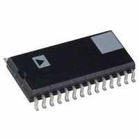
AD7244JR Analog Devices Inc, AD7244JR Datasheet - Page 11

AD7244JR
Manufacturer Part Number
AD7244JR
Description
IC DAC 14BIT LC2MOS DUAL 28SOIC
Manufacturer
Analog Devices Inc
Datasheet
1.AD7244JRZ.pdf
(12 pages)
Specifications of AD7244JR
Rohs Status
RoHS non-compliant
Settling Time
4µs
Number Of Bits
14
Data Interface
Serial
Number Of Converters
2
Voltage Supply Source
Dual ±
Power Dissipation (max)
205mW
Operating Temperature
-40°C ~ 85°C
Mounting Type
Surface Mount
Package / Case
28-SOIC (7.5mm Width)
Available stocks
Company
Part Number
Manufacturer
Quantity
Price
Part Number:
AD7244JR
Manufacturer:
ADI/亚德诺
Quantity:
20 000
Company:
Part Number:
AD7244JRZ
Manufacturer:
Analog Devices Inc
Quantity:
135
Part Number:
AD7244JRZ
Manufacturer:
ADI/亚德诺
Quantity:
20 000
REV. A
APPLYING THE AD7242/AD7244
Good printed circuit board layout is as important as the overall
circuit design itself in achieving high speed converter perfor-
mance. The AD7242 works on an LSB size of 1.465 mV, while
the AD7244 works on an LSB size of 366 V. Therefore, the
designer must be conscious of minimizing noise in both the
converter itself and in the surrounding circuitry. Switching
mode power supplies are not recommended as the switching
spikes can feed through to the on-chip amplifier. Other causes
of concern are ground loops and digital feedthrough from
microprocessors. These are factors that influence any high
performance converter, and a proper PCB layout that minimizes
these effects is essential for best performance.
LAYOUT HINTS
Ensure that the layout for the printed circuit board has separated
digital and analog lines as much as possible. Take care not to
run any digital track alongside an analog signal track. Establish a
single point analog ground (star ground) separate from the logic
system ground. Place this star ground as close as possible to the
AD7242/AD7244. Connect all analog grounds to this star
ground and also connect the AD7242/AD7244 DGND pins to
this ground. Do not connect any other digital grounds to this
analog ground point.
–11–
Low impedance analog and digital power supply common
returns are essential to low noise operation of high performance
converters. Therefore, the foil width for these tracks should be
kept as wide as possible. The use of ground planes minimizes
impedance paths and also guards the analog circuitry from
digital noise.
NOISE
Keep the signal leads on the V
signal return leads to AGND as short as possible to minimize
noise coupling. In applications where this is not possible, use a
shielded cable between the DAC outputs and their destination.
Reduce the ground circuit impedance as much as possible since
any potential difference in grounds between the DAC and its
destination device appears as an error voltage in series with the
DAC output.
OUTA
AD7242/AD7244
and V
OUTB
signals and the


