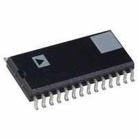
AD7244JR Analog Devices Inc, AD7244JR Datasheet - Page 9

AD7244JR
Manufacturer Part Number
AD7244JR
Description
IC DAC 14BIT LC2MOS DUAL 28SOIC
Manufacturer
Analog Devices Inc
Datasheet
1.AD7244JRZ.pdf
(12 pages)
Specifications of AD7244JR
Rohs Status
RoHS non-compliant
Settling Time
4µs
Number Of Bits
14
Data Interface
Serial
Number Of Converters
2
Voltage Supply Source
Dual ±
Power Dissipation (max)
205mW
Operating Temperature
-40°C ~ 85°C
Mounting Type
Surface Mount
Package / Case
28-SOIC (7.5mm Width)
Available stocks
Company
Part Number
Manufacturer
Quantity
Price
Part Number:
AD7244JR
Manufacturer:
ADI/亚德诺
Quantity:
20 000
Company:
Part Number:
AD7244JRZ
Manufacturer:
Analog Devices Inc
Quantity:
135
Part Number:
AD7244JRZ
Manufacturer:
ADI/亚德诺
Quantity:
20 000
REV. A
MICROPROCESSOR INTERFACING
Microprocessor interfacing to the AD7242/AD7244 is via a
serial bus that uses standard protocol compatible with DSP
processors and microcontrollers. The communication interface
consists of a separate transmit section for each of the DACs.
Each section has a clock signal, a data signal and a frame or
strobe pulse.
Figures 7 through 11 show the AD7242/AD7244 configured
for interfacing to a number of popular DSP processors and
microcontrollers.
AD7242/AD7244 to ADSP-2101/ADSP-2102 Interface
Figure 7 shows a serial interface between the AD7242/AD7244
and the ADSP-2101/ADSP-2102 DSP processor. The ADSP-
2101/ADSP-2102 has two serial ports and, in the interface
shown, both serial ports are used, one for each DAC. Both serial
ports do not have to be used; in the case where only one serial
port is used, an extra line (DACA/DACB as shown in the other
serial interfaces) would have to decode the one TFS line to
provide TFSA and TFSB lines for the AD7242/AD7244.
The three serial lines of the first serial port, SPORT1, of the
ADSP-2101/ADSP-2102 connect directly to the three serial
input lines of DACA of the AD7242/AD7244. The three serial
lines of SPORT2 connect directly to the three serial lines on the
DACB serial input port. Data from the ADSP-2101/ADSP-2102 is
valid on the falling edge of SCLK. A common LDAC signal is
used to drive the LDACA and LDACB inputs. This is shown to
be generated from a timer or clock recovery circuit but another
Figure 7. AD7242/AD7244 to ADSP-2101/ADSP-2102
Interface
–9–
control or address line of the ADSP-2101/ADSP-2102 could be
used to drive these inputs. Alternatively, the LDACA and
LDACB inputs of the AD7242/AD7244 could be hardwired
low; in this case the update of the DAC latches and analog
outputs takes place on the 16th falling edge of SCLK (after the
respective TFS signal goes low).
AD7242/AD7244 to DSP56000 Interface
A serial interface between the AD7242/AD7244 and the
DSP56000 is shown in Figure 8. The DSP56000 is configured
for normal mode, asynchronous operation with gated clock. It is
also set up for a 16-bit word with SCK and SC2 as outputs and
the FSL control bit set to a 0. SCK is internally generated on
the DSP56000 and applied to both the TCLKA and TCLKB
inputs of the AD7242/AD7244. Data from the DSP56000 is
valid on the falling edge of SCK. The serial data line, STD
drives the DTA and DTB serial input data lines of the
AD7242/AD7244.
The SC2 output provides the framing pulse for valid data. This
is an active high output and is gated with a DACA/DACB
control line before being applied to the TFSA and TFSB inputs
of the AD7242/AD7244. The DACA/DACB line determines
which DAC serial data is to be transferred to, i.e., which TFS
line is active when SC2 is active.
As in the previous interface, a common LDAC input is shown
driving the LDACA and LDACB inputs of the AD7242/AD7244.
Once again, these LDAC inputs could be hardwired low, in
which case V
falling edge of SCK after the TFSA or TFSB input goes low.
Figure 8. AD7242/AD7244 to DSP56000 Interface
OUTA
or V
OUTB
will be updated on the sixteenth
AD7242/AD7244


