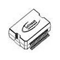
TLE6232GPNT Infineon Technologies, TLE6232GPNT Datasheet - Page 11

TLE6232GPNT
Manufacturer Part Number
TLE6232GPNT
Description
Manufacturer
Infineon Technologies
Datasheet
1.TLE6232GPNT.pdf
(19 pages)
Specifications of TLE6232GPNT
Switch Type
Low Side
Power Switch Family
TLE6232
Input Voltage
-0.3 to 7V
Power Switch On Resistance
250mOhm
Output Current
1.5A
Number Of Outputs
6
Mounting
Surface Mount
Supply Current
10mA
Package Type
DSO
Operating Temperature (min)
-40C
Operating Temperature (max)
150C
Operating Temperature Classification
Automotive
Pin Count
38
Power Dissipation
3300W
Lead Free Status / Rohs Status
Compliant
The MUX_REG and SCON_REG is writeable as well as readable from the micro controller.
The DIAG_REG can only be read from the µC.
This leads to five different control bytes which are recognized by the IC. The following table
shows the different modes.
WR_SCON
RD_SCON
WR_MUX
RD_MUX
RD_DIAG
Note:
All other possible control bytes will lead to an ignorance of the data bits, but the full diagnosis
information (like RD_DIAG command) is provided at the SO line. A reset of all fault registers
(and OT bit) the will only be done if the RD_DIAG command was clocked in.
Characteristics of the SPI Interface
If the slave select signal at CS is High or bit 7 and bit 6 of the instruction byte differ from „1“
and „0“, the state machine is set on default condition, i.e. the state machine expects an in-
struction.
If the 5V-reset (RESET) is active, the SPI output SO is switched into tristate.
In order to increase the possible number of SPI participants on one and the same CS signal,
bits 7 and 6 of the instruction byte are fixed as shown above. While receiving the first two bits
of the instruction byte the data output SO has to be in tristate. After having received the first
two bits TLE6232 has to decide if it is addressed (bit 7 = high, bit 6 = low). In this case the re-
maining 6 bits of the instruction byte and the data byte are accepted and the diagnostic feed-
back respectively the data byte content (MUX, SCON) is sent to the control-ler. Otherwise in-
struction and data bits are rejected and SO remains in tristate.
On a reading access the bit pattern of the data byte at the SPI input SI will be ignored. The
first SO byte sent out simultanously by the TLE 6232 GP always contains the common fault
bit, the overtemperature bit and the diagnostic information of channels 6 and 5 (2 bits each).
Depending on the SI control byte, the second SO byte contain the requested information.
V1
- DIAG_REG: 16-bit (2 byte) length. Contains the diagnostic information (2 bits per chan
nel), a common overtemperature bit and a common fault bit.
’X’ means ’don’t care’, because data will be ignored
’Dx’ represents the serial data bits, either being H (= OFF) or L (= ON)
’Mx’ enables parallel control of channel x H (=parallel) or L (=serial)
’Z’ means tristated
’F’ is the common fault flag
’OT’ is the common overtemperature flag
’DIAx’ is the 2 bit diagnosis information per channel
SI:
SO:
SI:
SO:
SI:
SO:
SI:
SO:
SI:
SO
MSB
Z Z F
Z Z F
Z Z F
Z Z F
Z Z F
H L L H H L X X
H L L H L H X X
H L H L H L X X
H L H L L H X X
H L L L L L X X
SI Control Byte
OT DIA6 DIA5
OT DIA6 DIA5
OT DIA6 DIA5
OT DIA6 DIA5
OT DIA6 DIA5
LSB
D6 D5 D4 D3 D2 D1 X X
X X X X X X X X
SCON6 .. . SCON1 H H
M6 M5 M4 M3 M2 M1 X X
DIA4
X
MUX6
X
DIA4
MSB
DIA4
Page
X
X
SI Data Byte
DIA3
DIA3
DIA3
X
X
. .
X
X
11
MUX1
DIA2
DIA2
DIA2
X
X
X
X
DIA1
DIA1
H H
DIA1
X
X
LSB
Data Sheet TLE 6232 GP
X
X
Write to SCON Register.
Read SCON Register
Write to MUX Register.
Read MUX Register
Read DIAG Register
24.Jan. 2002


