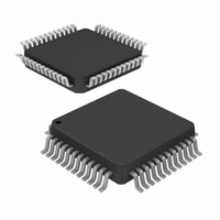
HI5728/6INZ Intersil, HI5728/6INZ Datasheet - Page 8

HI5728/6INZ
Manufacturer Part Number
HI5728/6INZ
Description
DAC DUAL 10-BIT 60MHZ 48-LQFP
Manufacturer
Intersil
Datasheet
1.HI5728IN.pdf
(19 pages)
Specifications of HI5728/6INZ
Settling Time
35ns
Number Of Bits
10
Data Interface
Parallel
Number Of Converters
2
Voltage Supply Source
Analog and Digital
Power Dissipation (max)
330mW
Operating Temperature
-40°C ~ 85°C
Mounting Type
Surface Mount
Package / Case
48-LQFP
Lead Free Status / RoHS Status
Lead free / RoHS Compliant
Available stocks
Company
Part Number
Manufacturer
Quantity
Price
Electrical Specifications
NOTES:
10. Measured with the clock at 60MSPS and the output frequency at 10MHz, both channels.
11. Parameters with MIN and/or MAX limits are 100% tested at +25°C, unless otherwise specified. Temperature limits established by characterization
Input Logic High Voltage with
3V Supply, V
Input Logic Low Voltage with
5V Supply, V
Input Logic Low Voltage with
3V Supply, V
Input Logic Current, I
Input Logic Current, I
Digital Input Capacitance, C
TIMING CHARACTERISTICS (Per Channel)
Data Setup Time, t
Data Hold Time, t
Propagation Delay Time, t
CLK Pulse Width, t
POWER SUPPLY CHARACTERISTICS
AVDD Power Supply
DVDD Power Supply
Analog Supply Current (I
Digital Supply Current (I
Supply Current (I
Power Dissipation
Power Supply Rejection
2. Gain Error measured as the error in the ratio between the full scale output current and the current through R
3. Limits established by characterization and are not production tested.
4. Spectral measurements made with differential coupled transformer and 100% amplitude.
5. Measured with the clock at 50MSPS and the output frequency at 1MHz, both channels.
6. Measured with the clock at 100MSPS and the output frequency at 40MHz, both channels.
7. See “Definition of Specifications” on page 16.
8. For operation below 3V, it is recommended that the output current be reduced to 12mA or less to maintain optimum performance. DV
9. For operation above 125MHz, it is recommended that the power supply be 3.3V or greater. The part is functional with the clock above 125MSPS
should be 32.
do not have to be equal.
and the power supply below 3.3V, but performance is degraded.
and are not production tested.
PARAMETER
IH
IL
IL
AVDD
HLD
SU
PW1
IH
IL
) Sleep Mode
, t
DVDD
AVDD
PW2
PD
IN
)
)
8
AV
per channel except for “POWER SUPPLY CHARACTERISTICS” on page 8 (Continued)
DD
(Note 3)
(Note 3)
(Note 3)
See Figure 41 (Note 3)
See Figure 41 (Note 3)
See Figure 41
See Figure 41 (Note 3)
(Notes 8, 9)
(Notes 8, 9)
(5V or 3V, IOUTFS = 20mA)
(5V or 3V, IOUTFS = 2mA)
(5V, IOUTFS = Don’t Care) (Note 5)
(3V, IOUTFS = Don’t Care) (Note 5)
(5V or 3V, IOUTFS = Don’t Care)
(5V, IOUTFS = 20mA) (Note 6)
(5V, IOUTFS = 2mA) (Note 6)
(3V, IOUTFS = 20mA) (Note 6)
(3V, IOUTFS = 2mA) (Note 6)
(5V, IOUTFS = 20mA) (Note 10)
(3.3V, IOUTFS = 20mA) (Note 10)
(3V, IOUTFS = 20mA) (Note 10)
Single Supply (Note 7)
= DV
DD
= +5V, V
REF
TEST CONDITIONS
= Internal 1.2V, IOUTFS = 20mA, T
HI5728
A
= +25°C for All Typical Values. Data given is
(Note 11) TYP
MIN
-0.2
-10
-10
T
2.1
2.7
2.7
3
3
4
A
-
-
-
-
-
-
-
-
-
-
-
-
-
-
-
-
SET
= -40°C TO +85°C
HI5728IN
(typically 625μA). Ideally the ratio
330
140
170
300
150
135
5.0
5.0
3.2
46
54
3
0
0
5
1
8
6
3
-
-
-
-
-
-
(Note 11)
MAX
+0.2
+10
+10
1.3
0.9
5.5
5.5
60
10
6
-
-
-
-
-
-
-
-
-
-
-
-
-
-
-
January 22, 2010
DD
% FSR/V
UNITS
and AV
mW
mW
mW
mW
mW
mW
mW
mA
mA
mA
mA
mA
µA
µA
pF
ns
ns
ns
ns
FN4321.5
V
V
V
V
V
DD


