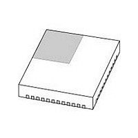
SC16C554BIBS NXP Semiconductors, SC16C554BIBS Datasheet - Page 10

SC16C554BIBS
Manufacturer Part Number
SC16C554BIBS
Description
Manufacturer
NXP Semiconductors
Datasheet
1.SC16C554BIBS.pdf
(58 pages)
Specifications of SC16C554BIBS
Transmit Fifo
16Byte
Receive Fifo
16Byte
Transmitter And Receiver Fifo Counter
Yes
Data Rate
5Mbps
Operating Supply Voltage (max)
5.5V
Mounting
Surface Mount
Pin Count
48
Operating Temperature (min)
-40C
Operating Temperature (max)
85C
Operating Temperature Classification
Industrial
Lead Free Status / Rohs Status
Compliant
NXP Semiconductors
Table 2.
SC16C554B_554DB
Product data sheet
Symbol
16/68
A0
A1
A2
A3
A4
CDA
CDB
CDC
CDD
CS
CSA
CSB
CSC
CSD
Pin description
Pin
PLCC68 LQFP64 LQFP80 HVQFN48
31
34
33
32
20
50
9
27
43
61
16
16
20
50
54
5.2 Pin description
-
24
23
22
-
-
64
18
31
49
-
7
11
38
42
-
48
47
46
-
-
19
42
59
2
-
28
33
68
73
All information provided in this document is subject to legal disclaimers.
5 V, 3.3 V and 2.5 V quad UART, 5 Mbit/s (max.) with 16-byte FIFOs
14
17
16
15
9
31
-
-
24
-
5
5
9
31
35
Rev. 4 — 8 June 2010
Type
I
I
I
I
I
I
I
I
I
I
I
I
I
I
I
Description
16/68 Interface type select (input with internal
pull-up). This input provides the 16 (Intel) or 68
(Motorola) bus interface type select. The functions of
IOR, IOW, INTA to INTD, and CSA to CSD are
re-assigned with the logic state of this pin. When this
pin is a logic 1, the 16 mode interface (16C554) is
selected. When this pin is a logic 0, the 68 mode
interface (68C554) is selected. When this pin is a
logic 0, IOW is re-assigned to R/W, RESET is
re-assigned to RESET, IOR is not used, and
INTA to INTD are connected in a wire-OR configuration.
The wire-OR outputs are connected internally to the
open-drain IRQ signal output. This pin is not available
on 64-pin packages which operate in the 16 mode only.
Address 0 select bit. Internal registers address
selection in 16 and 68 modes.
Address 1 select bit. Internal registers address
selection in 16 and 68 modes.
Address 2 select bit. Internal registers address
selection in 16 and 68 modes.
Address 3 to Address 4 select bits. When the 68
mode is selected, these pins are used to address or
select individual UARTs (providing CS is a logic 0). In
the 16 mode, these pins are re-assigned as chip
selects, see CSB and CSC.
Carrier Detect (active LOW). These inputs are
associated with individual UART channels A through D.
A logic 0 on this pin indicates that a carrier has been
detected by the modem for that channel.
Chip Select (active LOW). In the 68 mode, this pin
functions as a multiple channel chip enable. In this
case, all four UARTs (A to D) are enabled when the CS
pin is a logic 0. An individual UART channel is selected
by the data contents of address bits A3 to A4. when the
16 mode is selected (68-pin devices), this pin functions
as CSA (see definition under CSA, CSB).
Chip Select A, B, C, D (active LOW). This function is
associated with the 16 mode only, and for individual
channels ‘A’ through ‘D’. When in 16 mode, these pins
enable data transfers between the user CPU and the
SC16C554B/554DB for the channel(s) addressed.
Individual UART sections (A, B, C, D) are addressed by
providing a logic 0 on the respective CSA to CSD pin.
When the 68 mode is selected, the functions of these
pins are re-assigned. 68 mode functions are described
under their respective name/pin headings.
SC16C554B/554DB
© NXP B.V. 2010. All rights reserved.
10 of 58


