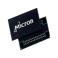
MT47H512M4HG-3:A Micron Technology Inc, MT47H512M4HG-3:A Datasheet - Page 23

MT47H512M4HG-3:A
Manufacturer Part Number
MT47H512M4HG-3:A
Description
Manufacturer
Micron Technology Inc
Type
DDR2 SDRAMr
Datasheet
1.MT47H512M4HG-3A.pdf
(134 pages)
Specifications of MT47H512M4HG-3:A
Organization
512Mx4
Address Bus
18b
Access Time (max)
450ps
Maximum Clock Rate
667MHz
Operating Supply Voltage (typ)
1.8V
Package Type
FBGA
Operating Temp Range
0C to 70C
Operating Supply Voltage (max)
1.9V
Operating Supply Voltage (min)
1.7V
Supply Current
170mA
Pin Count
60
Mounting
Surface Mount
Operating Temperature Classification
Commercial
Lead Free Status / Rohs Status
Compliant
- Current page: 23 of 134
- Download datasheet (10Mb)
FBGA Package Capacitance
Table 4: Input Capacitance
PDF: 09005aef824f87b6
2gbddr2.pdf – Rev. F 12/10 EN
Parameter
Input capacitance: CK, CK#
Delta input capacitance: CK, CK#
Input capacitance: BA[2:0], A[14:0] (A[13:0] on
x16), CS#, RAS#, CAS#, WE#, CKE, ODT
Delta input capacitance: Address balls, bank
address balls, CS#, RAS#, CAS#, WE#, CKE, ODT
Input/output capacitance: DQ, DQS, DM, NF
Delta input/output capacitance: DQ, DQS, DM,
NF
Notes:
1. This parameter is sampled. V
2. The capacitance per ball group will not differ by more than this maximum amount for
3. ΔC are not pass/fail parameters; they are targets.
4. Reduce MAX limit by 0.25pF for -3/-3E speed devices.
MHz, T
with I/O balls, reflecting the fact that they are matched in loading.
any given device.
C
= 25°C, V
Symbol
OUT(DC)
C
C
C
C
C
DCK
C
DIO
CK
DI
IO
I
= V
23
DD
DDQ
= +1.8V ±0.1V, V
/2, V
Min
1.0
1.0
2.5
Micron Technology, Inc. reserves the right to change products or specifications without notice.
–
–
–
OUT
(peak-to-peak) = 0.1V. DM input is grouped
2Gb: x4, x8, x16 DDR2 SDRAM
DDQ
Max
0.25
0.25
2.0
2.0
4.0
0.5
= +1.8V ±0.1V, V
© 2006 Micron Technology, Inc. All rights reserved.
Units
pF
pF
pF
pF
pF
pF
REF
= V
Packaging
SS
, f = 100
Notes
2, 3
2, 3
1, 4
2, 3
1
1
Related parts for MT47H512M4HG-3:A
Image
Part Number
Description
Manufacturer
Datasheet
Request
R

Part Number:
Description:
IC SDRAM 64MBIT 133MHZ 54TSOP
Manufacturer:
Micron Technology Inc
Datasheet:

Part Number:
Description:
IC SDRAM 64MBIT 5.5NS 86TSOP
Manufacturer:
Micron Technology Inc
Datasheet:

Part Number:
Description:
IC SDRAM 64MBIT 200MHZ 86TSOP
Manufacturer:
Micron Technology Inc
Datasheet:

Part Number:
Description:
IC SDRAM 64MBIT 133MHZ 54TSOP
Manufacturer:
Micron Technology Inc
Datasheet:

Part Number:
Description:
IC SDRAM 128MBIT 133MHZ 54TSOP
Manufacturer:
Micron Technology Inc
Datasheet:

Part Number:
Description:
IC SDRAM 256MBIT 133MHZ 90VFBGA
Manufacturer:
Micron Technology Inc
Datasheet:

Part Number:
Description:
IC SDRAM 128MBIT 133MHZ 54TSOP
Manufacturer:
Micron Technology Inc
Datasheet:

Part Number:
Description:
IC SDRAM 256MBIT 133MHZ 54TSOP
Manufacturer:
Micron Technology Inc
Datasheet:

Part Number:
Description:
IC DDR SDRAM 512MBIT 6NS 66TSOP
Manufacturer:
Micron Technology Inc
Datasheet:

Part Number:
Description:
IC SDRAM 128MBIT 167MHZ 86TSOP
Manufacturer:
Micron Technology Inc
Datasheet:

Part Number:
Description:
IC SDRAM 128MBIT 143MHZ 86TSOP
Manufacturer:
Micron Technology Inc
Datasheet:

Part Number:
Description:
SDRAM 256M-BIT 1.8V 54-PIN VFBGA
Manufacturer:
Micron Technology Inc
Datasheet:

Part Number:
Description:
IC SDRAM 128MBIT 143MHZ 86TSOP
Manufacturer:
Micron Technology Inc
Datasheet:

Part Number:
Description:
IC SDRAM 128MBIT 125MHZ 54VFBGA
Manufacturer:
Micron Technology Inc
Datasheet:

Part Number:
Description:
IC SDRAM 128MBIT 125MHZ 54VFBGA
Manufacturer:
Micron Technology Inc
Datasheet:


