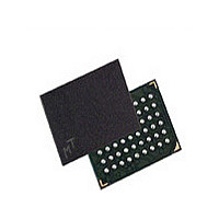
MT48H16M16LFBF-75 IT:G Micron Technology Inc, MT48H16M16LFBF-75 IT:G Datasheet - Page 51

MT48H16M16LFBF-75 IT:G
Manufacturer Part Number
MT48H16M16LFBF-75 IT:G
Description
Manufacturer
Micron Technology Inc
Type
Mobile SDRAMr
Datasheet
1.MT48H16M16LFBF-75_ITG.pdf
(86 pages)
Specifications of MT48H16M16LFBF-75 IT:G
Organization
16Mx16
Density
256Mb
Address Bus
15b
Access Time (max)
8/6ns
Maximum Clock Rate
133MHz
Operating Supply Voltage (typ)
1.8V
Package Type
VFBGA
Operating Temp Range
-40C to 85C
Operating Supply Voltage (max)
1.95V
Operating Supply Voltage (min)
1.7V
Supply Current
80mA
Pin Count
54
Mounting
Surface Mount
Operating Temperature Classification
Industrial
Lead Free Status / Rohs Status
Compliant
- Current page: 51 of 86
- Download datasheet (3Mb)
Figure 20: READ-to-WRITE With Extra Clock Cycle
Figure 21: READ-to-PRECHARGE
PDF: 09005aef834c13d2
256mb_mobile_sdram_y36n.pdf - Rev. I 11/09 EN
Note:
Note:
Command
Command
Command
Address
Address
Address
1. CL = 3. The READ command can be issued to any bank, and the WRITE command can be
1. DQM is LOW.
DQM
CLK
to any bank.
CLK
CLK
DQ
DQ
DQ
Bank a,
Bank a,
Bank,
T0
T0
Col n
T0
READ
Col n
READ
READ
Col
CL = 2
CL = 3
T1
T1
T1
256Mb: 16 Meg x 16, 8 Meg x 32 Mobile SDRAM
NOP
NOP
NOP
51
T2
T2
T2
NOP
NOP
NOP
D
OUT
Transitioning data
T3
T3
T3
Micron Technology, Inc. reserves the right to change products or specifications without notice.
NOP
NOP
NOP
D
D
D
t HZ
OUT
OUT
OUT
PRECHARGE
PRECHARGE
(a or all)
(a or all)
T4
T4
T4
Bank
Bank
NOP
X = 1 cycle
D
D
Transitioning data
OUT
OUT
X = 2 cycles
T5
T5
T5
Don’t Care
Bank,
WRITE
Col b
NOP
NOP
D
D
D
OUT
OUT
IN
t DS
t RP
t RP
©2008 Micron Technology, Inc. All rights reserved.
T6
T6
READ Operation
NOP
NOP
D
OUT
Don’t Care
ACTIVE
Bank a,
ACTIVE
Bank a,
T7
T7
Row
Row
Related parts for MT48H16M16LFBF-75 IT:G
Image
Part Number
Description
Manufacturer
Datasheet
Request
R

Part Number:
Description:
IC SDRAM 64MBIT 133MHZ 54TSOP
Manufacturer:
Micron Technology Inc
Datasheet:

Part Number:
Description:
IC SDRAM 64MBIT 5.5NS 86TSOP
Manufacturer:
Micron Technology Inc
Datasheet:

Part Number:
Description:
IC SDRAM 64MBIT 200MHZ 86TSOP
Manufacturer:
Micron Technology Inc
Datasheet:

Part Number:
Description:
IC SDRAM 64MBIT 133MHZ 54TSOP
Manufacturer:
Micron Technology Inc
Datasheet:

Part Number:
Description:
IC SDRAM 128MBIT 133MHZ 54TSOP
Manufacturer:
Micron Technology Inc
Datasheet:

Part Number:
Description:
IC SDRAM 256MBIT 133MHZ 90VFBGA
Manufacturer:
Micron Technology Inc
Datasheet:

Part Number:
Description:
IC SDRAM 128MBIT 133MHZ 54TSOP
Manufacturer:
Micron Technology Inc
Datasheet:

Part Number:
Description:
IC SDRAM 256MBIT 133MHZ 54TSOP
Manufacturer:
Micron Technology Inc
Datasheet:

Part Number:
Description:
IC DDR SDRAM 512MBIT 6NS 66TSOP
Manufacturer:
Micron Technology Inc
Datasheet:

Part Number:
Description:
IC SDRAM 128MBIT 167MHZ 86TSOP
Manufacturer:
Micron Technology Inc
Datasheet:

Part Number:
Description:
IC SDRAM 128MBIT 143MHZ 86TSOP
Manufacturer:
Micron Technology Inc
Datasheet:

Part Number:
Description:
SDRAM 256M-BIT 1.8V 54-PIN VFBGA
Manufacturer:
Micron Technology Inc
Datasheet:

Part Number:
Description:
IC SDRAM 128MBIT 143MHZ 86TSOP
Manufacturer:
Micron Technology Inc
Datasheet:

Part Number:
Description:
IC SDRAM 128MBIT 125MHZ 54VFBGA
Manufacturer:
Micron Technology Inc
Datasheet:

Part Number:
Description:
IC SDRAM 128MBIT 125MHZ 54VFBGA
Manufacturer:
Micron Technology Inc
Datasheet:


