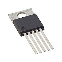
FSCM0565RCYDTU_NL Fairchild Semiconductor, FSCM0565RCYDTU_NL Datasheet - Page 11

FSCM0565RCYDTU_NL
Manufacturer Part Number
FSCM0565RCYDTU_NL
Description
Manufacturer
Fairchild Semiconductor
Datasheet
1.FSCM0565RCYDTU_NL.pdf
(20 pages)
Specifications of FSCM0565RCYDTU_NL
Power Switch Family
FSCM0565R
Power Switch On Resistance
1.76Ohm
Output Current
2.5A
Number Of Outputs
Single
Mounting
Through Hole
Supply Current
2.5mA
Package Type
TO-220
Operating Temperature (min)
-25C
Operating Temperature (max)
85C
Operating Temperature Classification
Commercial
Pin Count
5 +Tab
Power Dissipation
120W
Lead Free Status / Rohs Status
Compliant
FSCM0565R
current spike through the SenseFET, caused by primary-side
capacitance and secondary-side rectifier reverse recovery.
Excessive voltage across the Rsense resistor can lead to
incorrect feedback operation in the current mode PWM
control. To counter this effect, the FSCM0565R employs a
leading edge blanking (LEB) circuit. This circuit inhibits the
PWM comparator for a short time (T
is turned on.
3. Protection Circuit: The FSCM0565R has several self
protective functions such as over load protection (OLP), over
voltage protection (OVP) and thermal shutdown (TSD).
Because these protection circuits are fully integrated into the
IC without external components, the reliability can be
improved without increasing cost. Once the fault condition
occurs, switching is terminated and the SenseFET remains
off. This causes Vcc to fall. When Vcc reaches the UVLO
stop voltage of 8V, the current consumed by the
FSCM0565R decreases to the startup current (typically
25uA) and the current supplied from the DC link charges the
external capacitor (C
When Vcc reaches the start voltage of 12V, the FSCM0565R
resumes its normal operation. In this manner, the auto-restart
can alternately enable and disable the switching of the power
SenseFET until the fault condition is eliminated (see Figure
19).
3.1 Over Load Protection (OLP): Overload is defined as
the load current exceeding a pre-set level due to an
unexpected event. In this situation, the protection circuit
should be activated to protect the SMPS. However, even
when the SMPS is in the normal operation, the over load
protection circuit can be activated during the load transition.
To avoid this undesired operation, the over load protection
circuit is designed to be activated after a specified time to
11
Vds
Vcc
12V
8V
Power
On
Figure 19. Auto Restart Operation
Operation
Normal
a
) that is connected to the Vcc pin.
occurs
Fault
Situation
Fault
LEB
removed
Fault
) after the SenseFET
Operation
Normal
t
determine whether it is a transient situation or an overload
situation. Because of the pulse-by-pulse current limit
capability, the maximum peak current through the SenseFET
is limited, and therefore the maximum input power is
restricted with a given input voltage. If the output consumes
beyond this maximum power, the output voltage (Vo)
decreases below the set voltage. This reduces the current
through the opto-coupler LED, which also reduces the opto-
coupler transistor current, thus increasing the feedback
voltage (Vfb). If Vfb exceeds 2.5V, D1 is blocked and the
5.3uA current source (I
Vcc. In this condition, Vfb continues increasing until it
reaches 6V, when the switching operation is terminated as
shown in Figure 20. The delay time for shutdown is the time
required to charge C
In general, a 10 ~ 50 ms delay time is typical for most
applications.
3.2 Over Voltage Protection (OVP): If the secondary side
feedback circuit were to malfunction or a solder defect
caused an open in the feedback path, the current through the
opto-coupler transistor becomes almost zero. Then, Vfb
climbs up in a similar manner to the over load situation,
forcing the preset maximum current to be supplied to the
SMPS until the over load protection is activated. Because
more energy than required is provided to the output, the
output voltage may exceed the rated voltage before the over
load protection is activated, resulting in the breakdown of the
devices in the secondary side. To prevent this situation, an
over voltage protection (OVP) circuit is employed. In
general, Vcc is proportional to the output voltage and the
FSCM0565R uses Vcc instead of directly monitoring the
output voltage. If V
activated resulting in the termination of the switching
operation. To avoid undesired activation of OVP during
normal operation, Vcc should be designed to be below 19V.
3.3 Thermal Shutdown (TSD): The SenseFET and the
6.0V
2.5V
V
FB
Figure 20. Over Load Protection
T
1
B
CC
from 2.5V to 6.0V with 5.3uA (I
delay
Over Load Protection
T
12
exceeds 19V, an OVP circuit is
= Cfb*(6.0-2.5)/I
) starts to charge C
delay
B
slowly up to
T
2
delay
t
).


