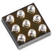
LM4673TM National Semiconductor, LM4673TM Datasheet - Page 4

LM4673TM
Manufacturer Part Number
LM4673TM
Description
AUDIO AMP, MONO CLASS D, POWERWISE
Manufacturer
National Semiconductor
Datasheet
1.LM4673TM.pdf
(24 pages)
Specifications of LM4673TM
Operational Class
Class-D
Audio Amplifier Output Configuration
1-Channel Mono
Output Power (typ)
2.65x1@4OhmW
Audio Amplifier Function
Speaker
Total Harmonic Distortion
0.03@8Ohm@0.1W%
Single Supply Voltage (typ)
3/5V
Dual Supply Voltage (typ)
Not RequiredV
Power Supply Requirement
Single
Rail/rail I/o Type
No
Power Supply Rejection Ratio
78dB
Single Supply Voltage (min)
2.4V
Single Supply Voltage (max)
5.5V
Dual Supply Voltage (min)
Not RequiredV
Dual Supply Voltage (max)
Not RequiredV
Operating Temp Range
-40C to 85C
Operating Temperature Classification
Industrial
Mounting
Surface Mount
Pin Count
9
Package Type
uSMD
Amplifier Class
D
No. Of Channels
1
Output Power
2.65W
Supply Voltage Range
2.4V To 5.5V
Thd + N
0.03% @ 100mW, VDD=5V
Load Impedance
4ohm
Operating Temperature Range
-40°C To +85°C
Rohs Compliant
Yes
Lead Free Status / Rohs Status
Not Compliant
Available stocks
Company
Part Number
Manufacturer
Quantity
Price
Part Number:
LM4673TM
Manufacturer:
NS/国半
Quantity:
20 000
Part Number:
LM4673TMX
Manufacturer:
NS/国半
Quantity:
20 000
Part Number:
LM4673TMX/NOPB
Manufacturer:
TI/德州仪器
Quantity:
20 000
www.national.com
|V
|I
|I
I
I
V
V
R
A
R
P
DD
SD
Symbol
IH
IL
SDIH
SDIL
V
O
OSD
SD
OS
Absolute Maximum Ratings
If Military/Aerospace specified devices are required,
please contact the National Semiconductor Sales Office/
Distributors for availability and specifications.
Supply Voltage (Note 1)
Storage Temperature
Voltage at Any Input Pin
Power Dissipation (Note 3)
ESD Susceptibility, all other pins (Note 4)
ESD Susceptibility (Note 5)
Junction Temperature (T
Electrical Characteristics
The following specifications apply for A
T
|
|
A
|
= 25°C.
Differential Output Offset Voltage
Logic High Input Current
Logic Low Input Current
Quiescent Power Supply Current
Shutdown Current
Shutdown voltage input high
Shutdown voltage input low
Output Impedance
Gain
Resistance from Shutdown Pin to
GND
Output Power
Parameter
JMAX
)
V
DD
+ 0.3V
V
= 2V/V (R
−65°C to +150°C
≥
Internally Limited
(Notes 1, 2)
V
≥
V
V
V
V
V
V
V
V
V
V
V
V
V
R
THD = 10% (max)
f = 1kHz, 22kHz BW
V
V
V
R
THD = 1% (max)
f = 1kHz, 22kHz BW
V
V
V
(Notes 1, 2)
GND - 0.3V
I
DD
DD
DD
IN
IN
IN
IN
IN
IN
SHUTDOWN
DD
SHUTDOWN
DD
DD
DD
DD
DD
DD
L
L
I
= 0V, A
= 15μH + 4Ω + 15μH
= 15μH + 4Ω + 15μH
= 150kΩ), R
= 0V, No Load, V
= 0V, No Load, V
= 0V, No Load, V
= 0V, R
= 0V, R
= 0V, R
= 2.4V to 5.0V
= 5.0V, V
= 5.0V, V
= 2.4V to 5.0V
= 5V
= 3.6V
= 2.5V
= 5V
= 3.6V
= 2.5V
150°C
2.0kV
200V
6.0V
V
L
L
L
= 0V
= 0.4V
= 2V/V,
Conditions
= 8Ω, V
= 8Ω, V
= 8Ω, V
I
I
= 5.5V
= –0.3V
L
4
= 15µH + 8Ω + 15µH unless otherwise specified. Limits apply for
Thermal Resistance
θ
θ
Soldering Information
See AN-1112 "microSMD Wafers Level Chip Scale
Package."
Operating Ratings
Temperature Range
Supply Voltage
DD
DD
DD
DD
DD
DD
T
= 5.0V
= 3.6V
= 2.4V
= 5.0V
= 3.6V
= 2.4V
JA
JA
MIN
(micro SMD)
(LLP)
≤
T
A
≤
T
MAX
300kΩ/R
(Note 6)
Typical
0.01
2.65
2.15
1.06
100
300
550
450
0.9
2.6
2.1
1.7
2.6
2.1
1.7
1.3
17
5
LM4673
I
(Notes 1, 2)
(Notes 7, 8)
270kΩ/R
330kΩ/R
Limit
3.75
100
2.9
2.3
1.4
0.4
5
1
−40°C
2.4V
I
I
≤
≤
V
T
V/V (max)
99.1°C/W
DD
mV (max)
mA (max)
mA (max)
V/V (min)
μA (max)
μA (max)
μA (max)
(Limits)
A
V (max)
V (min)
73°C/W
Units
≤
≤
mW
mW
mA
kΩ
kΩ
W
W
W
W
85°C
5.5V


