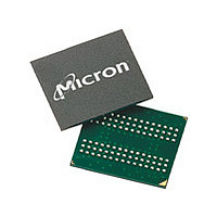
MT46H16M32LFCM-6 IT:B Micron Technology Inc, MT46H16M32LFCM-6 IT:B Datasheet - Page 59

MT46H16M32LFCM-6 IT:B
Manufacturer Part Number
MT46H16M32LFCM-6 IT:B
Description
Manufacturer
Micron Technology Inc
Type
DDR SDRAMr
Datasheet
1.MT46H16M32LFCM-6_ITB.pdf
(98 pages)
Specifications of MT46H16M32LFCM-6 IT:B
Organization
16Mx32
Density
512Mb
Address Bus
15b
Access Time (max)
6.5/5ns
Maximum Clock Rate
166MHz
Operating Supply Voltage (typ)
1.8V
Package Type
VFBGA
Operating Temp Range
-40C to 85C
Operating Supply Voltage (max)
1.95V
Operating Supply Voltage (min)
1.7V
Supply Current
115mA
Pin Count
90
Mounting
Surface Mount
Operating Temperature Classification
Industrial
Lead Free Status / Rohs Status
Compliant
- Current page: 59 of 98
- Download datasheet (4Mb)
Bank/Row Activation
PDF: 09005aef82d5d305
512mb_ddr_mobile_sdram_t47m.pdf – Rev. I 12/09 EN
Before any READ or WRITE commands can be issued to a bank within the device, a row
in that bank must be opened. This is accomplished via the ACTIVE command, which
selects both the bank and the row to be activated (see Figure 10 (page 37)). After a row is
opened with the ACTIVE command, a READ or WRITE command can be issued to that
row, subject to the
A subsequent ACTIVE command to a different row in the same bank can only be issued
after the previous active row has been precharged. The minimum time interval between
successive ACTIVE commands to the same bank is defined by
A subsequent ACTIVE command to another bank can be issued while the first bank is
being accessed, which results in a reduction of total row access overhead. The mini-
mum time interval between successive ACTIVE commands to different banks is defined
by
t
RRD.
t
RCD specification.
59
512Mb: x16, x32 Mobile LPDDR SDRAM
Micron Technology, Inc. reserves the right to change products or specifications without notice.
Bank/Row Activation
© 2004 Micron Technology, Inc. All rights reserved.
t
RC.
Related parts for MT46H16M32LFCM-6 IT:B
Image
Part Number
Description
Manufacturer
Datasheet
Request
R

Part Number:
Description:
IC SDRAM 64MBIT 133MHZ 54TSOP
Manufacturer:
Micron Technology Inc
Datasheet:

Part Number:
Description:
IC SDRAM 64MBIT 5.5NS 86TSOP
Manufacturer:
Micron Technology Inc
Datasheet:

Part Number:
Description:
IC SDRAM 64MBIT 200MHZ 86TSOP
Manufacturer:
Micron Technology Inc
Datasheet:

Part Number:
Description:
IC SDRAM 64MBIT 133MHZ 54TSOP
Manufacturer:
Micron Technology Inc
Datasheet:

Part Number:
Description:
IC SDRAM 128MBIT 133MHZ 54TSOP
Manufacturer:
Micron Technology Inc
Datasheet:

Part Number:
Description:
IC SDRAM 256MBIT 133MHZ 90VFBGA
Manufacturer:
Micron Technology Inc
Datasheet:

Part Number:
Description:
IC SDRAM 128MBIT 133MHZ 54TSOP
Manufacturer:
Micron Technology Inc
Datasheet:

Part Number:
Description:
IC SDRAM 256MBIT 133MHZ 54TSOP
Manufacturer:
Micron Technology Inc
Datasheet:

Part Number:
Description:
IC DDR SDRAM 512MBIT 6NS 66TSOP
Manufacturer:
Micron Technology Inc
Datasheet:

Part Number:
Description:
IC SDRAM 128MBIT 167MHZ 86TSOP
Manufacturer:
Micron Technology Inc
Datasheet:

Part Number:
Description:
IC SDRAM 128MBIT 143MHZ 86TSOP
Manufacturer:
Micron Technology Inc
Datasheet:

Part Number:
Description:
SDRAM 256M-BIT 1.8V 54-PIN VFBGA
Manufacturer:
Micron Technology Inc
Datasheet:

Part Number:
Description:
IC SDRAM 128MBIT 143MHZ 86TSOP
Manufacturer:
Micron Technology Inc
Datasheet:

Part Number:
Description:
IC SDRAM 128MBIT 125MHZ 54VFBGA
Manufacturer:
Micron Technology Inc
Datasheet:

Part Number:
Description:
IC SDRAM 128MBIT 125MHZ 54VFBGA
Manufacturer:
Micron Technology Inc
Datasheet:


